
- Home
- »
- Advanced Interior Materials
- »
-
Semiconductor Cleaning Equipment Market Report, 2033GVR Report cover
![Semiconductor Cleaning Equipment Market (2026 - 2033)Report]()
Semiconductor Cleaning Equipment Market (2026 - 2033)
Size, Share & Trends Analysis Report By Product (Single Wafer Cleaning Equipment, Batch-type Cleaning Equipment, Spin Scrubbers), By Wafer Size (300 mm, 200 mm, less than 150 mm), By End Use, By Application, By Region And Segment Forecasts
Market Size, 2025
$6.4BMarket Estimate, 2026
$7.8BMarket Forecast, 2033
$17.1BCAGR, 2026–2033
11.9%Semiconductor Cleaning Equipment Market Summary
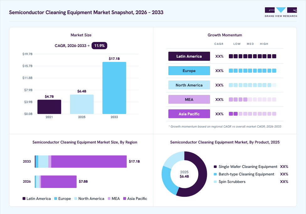
The global semiconductor cleaning equipment market size was valued at USD 6.4 billion in 2025 and is projected to grow from USD 7.8 billion in 2026 to USD 17.1 billion by 2033, at a CAGR of 11.9% from 2026 to 2033. Asia Pacific dominated the market, accounting for the largest revenue share of 86.6% in 2025. The market is driven by the increasing complexity of semiconductor fabrication, the expansion of wafer manufacturing capacity, and stringent requirements for wafer surface cleanliness.
Key Market Trends & Insights
- By product: Batch-type cleaning equipment segment is projected to grow at 12.4% CAGR during forecast period.
- By wafer size: 200 mm segment is expected to grow at a CAGR of 11.7% from 2026 to 2033.
- By application: Front-end-of-line (FEOL) dominated the market in 2025 accounting for 61.9% market share.
- By end use: Logic is projected to register a growing CAGR of 11.7% during the forecast period.
Regional Highlights
- Largest regional market: Asia Pacific (86.6% revenue share, 2025)
- Fastest-growing regional market: Latin America (highest CAGR, 2026-2033)
- By country: Taiwan held the largest market share in 2025.
Market Size & Forecast
- Market size in 2025: USD 6.4 Billion
- Estimated market size in 2026: USD 7.8 Billion
- Projected market size by 2033: USD 17.1 Billion
- CAGR (2026-2033): 11.9%
Three ways to get this report
Buy it, customize it, or ask a question.Get the Full Report
What the study covers
- FormatsPDF · Excel · Dashboard
- Timeline2026–2033 annual, 2025 base
- Coverage20+ countries, 5 regions
- Companies10+ key players profiled
Customize the Report
20% free customization
- IncludeCountries, segments, points
- TailorTo your product definition
- ExtendDeeper competitor detail
- OrA fully bespoke study
- Turnaround5–10 working days
Ask Prism AI
A cited answer in seconds
- Corpus30K studies, 1.2M points
- ScopeAll markets, not just this
- CitationTraced to report & table
- HonestySays "not covered" if so
- SpeedSeconds, not days
As semiconductor manufacturers move toward smaller technology nodes and more advanced device architectures, tighter contamination control is required to minimize defects and maintain production yields, increasing demand for high-precision cleaning systems. The growing number of process steps and higher wafer-processing intensity are also creating greater requirements for reliable and efficient cleaning equipment across fabrication stages.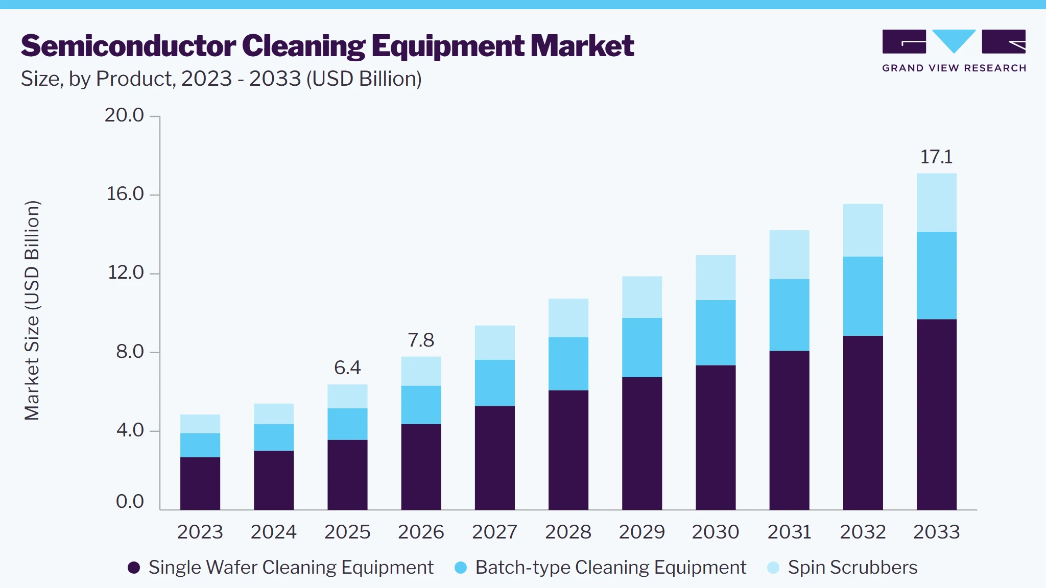
Investments in new semiconductor fabs, production-line expansions, technology upgrades, and modernization of existing facilities are generating opportunities for equipment suppliers, while the replacement of aging systems is contributing to recurring capital expenditure. Growing production of memory, logic, and foundry-based semiconductors, along with the expansion of advanced packaging and wafer-level processing, is broadening equipment requirements across different manufacturing applications.
Market Dynamics
The global semiconductor cleaning equipment market is influenced by semiconductor production volumes, fabrication process complexity, technology-node transitions, and capital investments in wafer manufacturing. Market development is shaped by requirements for stringent contamination control, precise wafer surface treatment, higher processing efficiency, and consistent cleaning performance. Purchasing decisions are also affected by equipment costs, qualification timelines, production-line integration, and technological requirements, while advances in cleaning processes and automation continue to create opportunities for equipment suppliers.
The transition toward smaller technology nodes and increasingly complex semiconductor architectures is increasing the number and precision of cleaning steps required during wafer fabrication. Tighter contamination-control requirements necessitate equipment capable of removing particles, residues, and other impurities while maintaining wafer integrity. This trend is increasing demand for cleaning systems offering greater process precision, cleaning uniformity, throughput, and automation.
Advanced semiconductor cleaning equipment involves substantial capital expenditure, which can influence purchasing decisions based on production requirements, utilization levels, and investment priorities. New systems also undergo extensive testing, qualification, and process integration before deployment in production environments. These requirements can lengthen procurement cycles and delay the adoption of new equipment.
Expansion of semiconductor fabrication capacity is creating opportunities for cleaning equipment manufacturers through new fabs, production-line additions, technology upgrades, and advanced-node manufacturing projects. Replacement of older systems and modernization of existing facilities also provide avenues for equipment sales as manufacturers seek improved automation, process control, throughput, and contamination management. This creates scope for suppliers offering equipment aligned with evolving wafer fabrication requirements.
Market Concentration & Characteristics
The semiconductor cleaning equipment market is characterized by a technologically specialized and relatively concentrated supplier structure, with established manufacturers offering equipment based on different wafer cleaning methods, system configurations, and processing requirements. Competitive differentiation is shaped by cleaning efficiency, surface uniformity, particle removal capability, wafer handling precision, throughput, automation, equipment reliability, and compatibility with different wafer sizes.
The industry is closely associated with the global semiconductor fabrication landscape, with market activity concentrated in regions possessing substantial wafer manufacturing capacity. Asia Pacific maintains a strong position owing to its extensive base of foundries, memory manufacturers, logic producers, and integrated device manufacturers, while North America and Europe continue to strengthen their semiconductor production capabilities through new fabrication facilities and capacity expansion initiatives.
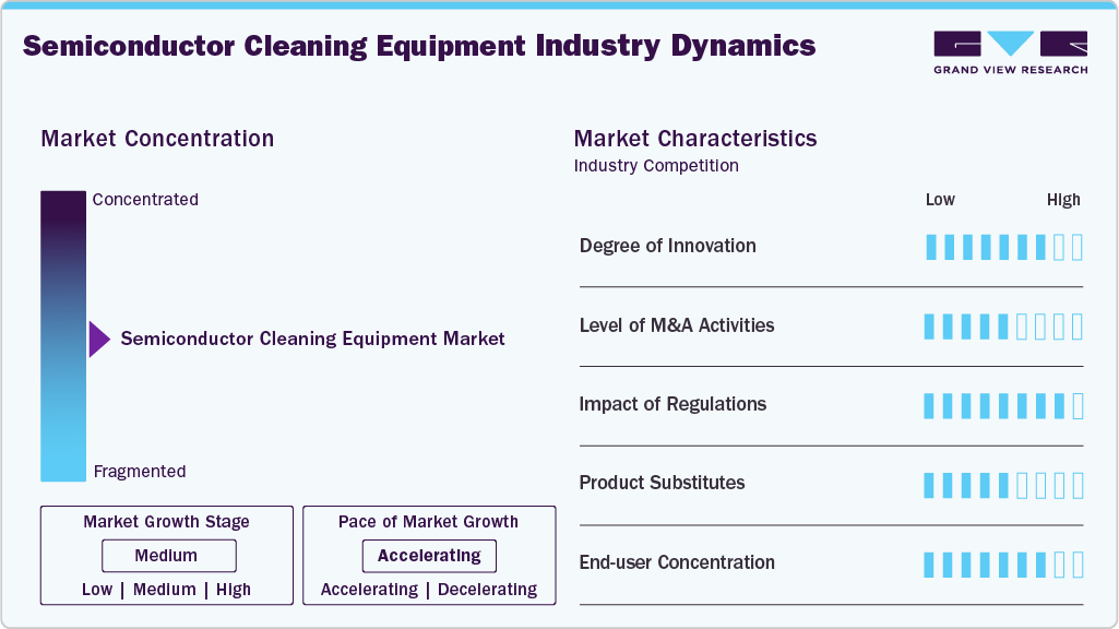
The market has substantial barriers to entry, reflecting high research and development requirements, specialized engineering expertise, stringent equipment qualification procedures, and the need for reliable performance within semiconductor manufacturing environments. Equipment typically undergoes extensive customer evaluation and process validation before deployment in production, making technical credibility and established supplier relationships important competitive considerations. Manufacturers must also continuously enhance equipment capabilities to address higher wafer throughput, tighter contamination-control requirements, increasingly complex fabrication processes, and transitions toward advanced semiconductor technologies.
Analyst Perspective
The semiconductor cleaning equipment market is expected to maintain steady growth as semiconductor manufacturers expand wafer fabrication capacity and adopt increasingly complex process technologies. The transition toward smaller technology nodes is intensifying requirements for wafer cleanliness, contamination control, and process precision, creating demand for advanced cleaning systems with higher automation and processing efficiency. New fab construction, capacity expansions, technology upgrades, and replacement of aging equipment will remain important contributors to equipment purchases across foundries, memory manufacturers, logic producers, and IDMs. Asia Pacific is expected to remain the largest regional market, supported by its established semiconductor manufacturing ecosystem and continued investments in wafer fabrication, while North America and Europe present additional opportunities through ongoing efforts to strengthen domestic semiconductor production. Overall, technological advancement and sustained fab investment are likely to remain the principal factors shaping competitive and revenue opportunities in the market.
Product Insights
The single wafer cleaning equipment segment accounted for the largest revenue share of 55.9% in 2025, driven by its ability to process wafers individually with precise control over cleaning conditions. These systems are well suited to fabrication processes requiring tight control of particle and residue removal, particularly as semiconductor device structures become increasingly complex. Their flexibility in adjusting cleaning parameters for individual wafers also makes them suitable for advanced manufacturing applications where process consistency and surface quality are critical.
The batch-type cleaning equipment segment is projected to register the fastest CAGR during the forecast period, supported by its ability to process multiple wafers simultaneously and accommodate high-volume manufacturing requirements. Batch processing can improve equipment utilization and processing efficiency where large numbers of wafers require similar cleaning treatments. Demand is also supported by applications where throughput and cost-efficient wafer processing are important considerations, particularly across established semiconductor production lines.
Wafer Size Insights
The 300 mm wafers segment accounted for the largest revenue share of 72.9% in 2025, reflecting their extensive use in high-volume semiconductor manufacturing. Cleaning equipment designed for 300 mm wafers is widely integrated into advanced fabrication environments where consistent surface preparation and high production efficiency are required. The large installed base of 300 mm wafer-processing facilities therefore contributes substantially to equipment revenue within this segment.
The 200 mm wafers segment is projected to register a growing CAGR during the forecast period, supported by continued production of mature-node and specialty semiconductors. Demand for 200 mm-compatible cleaning systems is also associated with applications such as power devices, sensors, analog components, and other established semiconductor technologies. Continued utilization of existing 200 mm fabrication capacity creates opportunities for equipment replacement, process upgrades, and cleaning system modernization.
End Use Insights
The foundry segment accounted for the largest revenue share of 34.0% in 2025, reflecting the substantial use of wafer cleaning equipment across contract semiconductor manufacturing operations. Foundries process wafers for multiple customers and device categories, creating demand for cleaning systems across diverse fabrication requirements. The need to maintain consistent wafer surface conditions across high-volume production lines contributes to equipment demand within this segment.
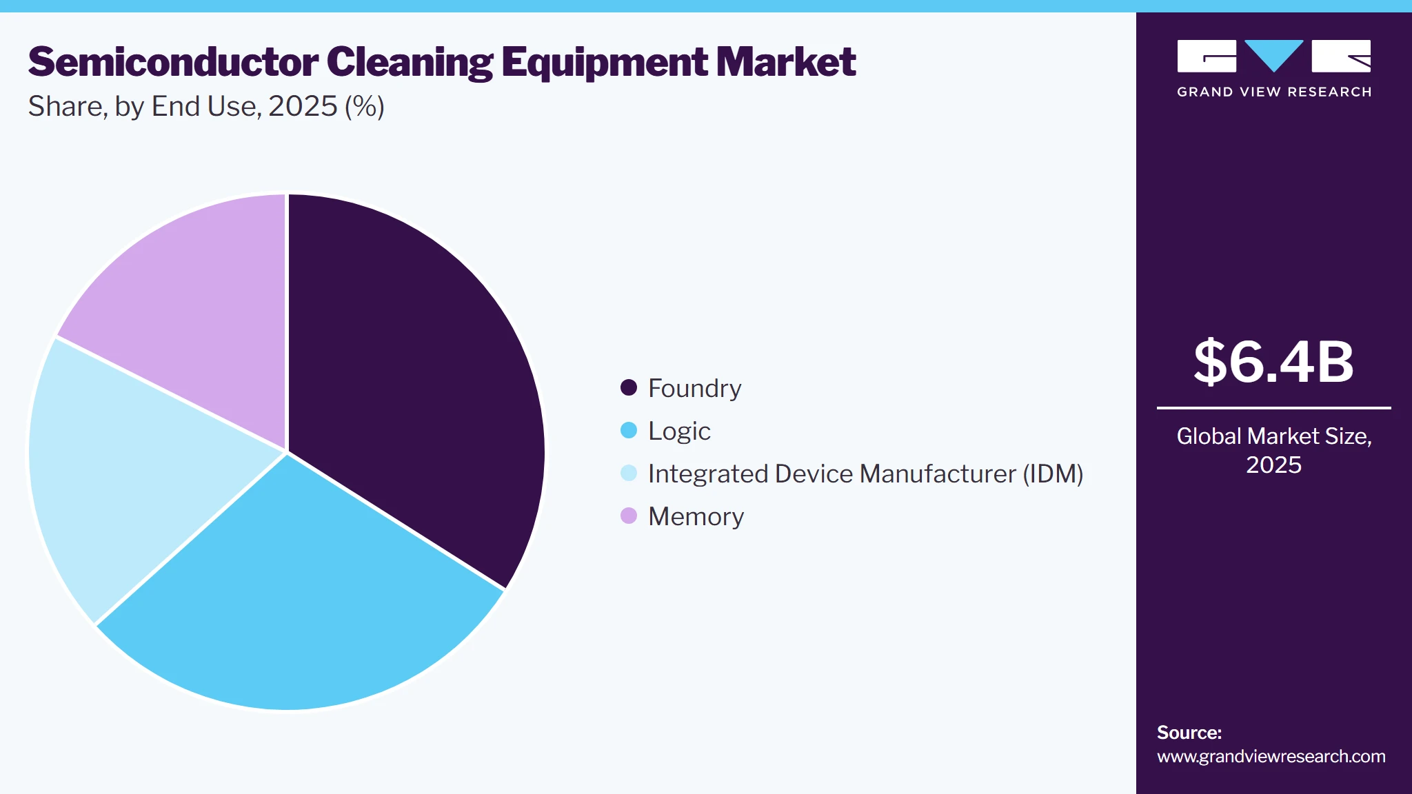
The logic segment is projected to register a growing CAGR during the forecast period, supported by increasing production of processors, microcontrollers, ASICs, and other logic devices. Increasing device complexity and tighter fabrication requirements are creating greater demand for controlled wafer-cleaning processes throughout logic semiconductor manufacturing. Expansion of advanced logic production is also creating opportunities for cleaning equipment compatible with increasingly sophisticated fabrication processes.
Application Insights
The front-end-of-line (FEOL) segment accounted for the largest revenue share in 2025, reflecting the substantial demand for cleaning equipment used during wafer fabrication and transistor formation. Cleaning systems at the FEOL stage remove particles, residues, and other contaminants from wafer surfaces between processing steps. The extensive number of cleaning requirements across FEOL operations contributes to equipment demand within this application.
The back-end-of-line (BEOL) segment is projected to register a CAGR of 11.7% during the forecast period, supported by increasing requirements for cleaning equipment during interconnect and multilayer wafer processing. Equipment used in BEOL applications is required to remove process residues and contaminants while maintaining wafer surface conditions. Increasing adoption of advanced semiconductor structures is creating further requirements for dedicated cleaning systems in BEOL applications.
Regional Insights
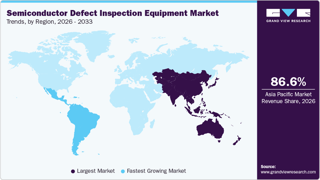
Asia Pacific accounted for 86.6% of the global semiconductor cleaning equipment market revenue in 2025, reflecting the region’s concentration of semiconductor fabrication capacity and extensive wafer-processing activities. The presence of foundries, memory manufacturers, logic producers, and IDMs creates substantial equipment requirements across different production stages and wafer sizes. The region’s combination of established manufacturing facilities and ongoing capacity development supports demand for new cleaning systems as well as replacement and process-upgrade equipment.
Taiwan Semiconductor Cleaning Equipment Market Trends
Taiwan is the largest market in the Asia Pacific semiconductor cleaning equipment market, driven by its highly developed semiconductor manufacturing ecosystem and strong concentration of leading-edge wafer fabrication facilities. The country is a major global hub for foundry manufacturing, with extensive production of advanced logic and specialty semiconductors, generating substantial demand for wafer cleaning equipment across multiple stages of semiconductor processing. Continuous investments in advanced process nodes, fabrication capacity expansion, and semiconductor manufacturing technologies are further increasing the requirement for high-precision cleaning systems.
China accounted for 22.4% of the Asia Pacific semiconductor cleaning equipment market revenue in 2025, making it the second-largest market in the region. The country has a well-established semiconductor manufacturing base spanning foundry, memory, power, and specialty devices, creating demand for cleaning systems across a broad range of wafer-processing operations. Continued expansion of domestic semiconductor fabrication capacity, alongside investments in localized semiconductor supply chains and advanced manufacturing capabilities, is further supporting the installation and upgrading of semiconductor cleaning equipment..
The India semiconductor cleaning equipment market is witnessing growth. The country is developing its semiconductor manufacturing ecosystem alongside its expanding electronics and semiconductor design industries. The emergence of domestic wafer fabrication and semiconductor production projects is creating an initial need for front-end processing equipment, including wafer-cleaning systems. Demand is likely to be shaped by the commissioning of new facilities, production scale, and the types of semiconductor devices manufactured locally. As domestic fabrication capabilities develop, opportunities for cleaning equipment suppliers are expected to broaden across installation, process development, and subsequent equipment replacement.
North America Semiconductor Cleaning Equipment Market Trends
North America has an established semiconductor cleaning equipment market, supported by its semiconductor manufacturing, research, and technology ecosystem. Demand for cleaning systems is associated with wafer fabrication for logic, memory, power, and specialty semiconductor devices, where controlled wafer surfaces are required throughout fabrication. Increasing process complexity is creating requirements for equipment capable of achieving consistent cleaning performance across different manufacturing stages. The region also has an installed base of semiconductor fabrication facilities that generates replacement and equipment upgrade requirements.
The U.S. has a well-developed semiconductor manufacturing ecosystem spanning foundries, IDMs, logic, memory, and specialty semiconductor production. Demand for cleaning equipment is influenced by the development of advanced semiconductor manufacturing processes and the requirements of high-volume wafer fabrication. Expansion of domestic semiconductor production is creating opportunities for new equipment installations, while existing facilities generate demand for replacement and upgraded systems.
The Canada semiconductor cleaning equipment market is growing because of the activities spanning compound semiconductors, photonics, sensors, research, and advanced electronics. These applications require controlled wafer-processing environments and cleaning systems suited to specialized materials and production processes. Research and development activities also generate requirements for precision wafer-processing equipment in laboratory, pilot-scale, and specialized manufacturing settings.
Europe Semiconductor Cleaning Equipment Market Trends
Europe has a diversified semiconductor manufacturing ecosystem encompassing automotive electronics, power semiconductors, industrial devices, sensors, and specialty technologies. This production mix creates demand for cleaning equipment across different wafer-processing requirements and fabrication environments. Semiconductor manufacturers require controlled cleaning processes to maintain surface quality and process consistency during device production. Equipment demand is also influenced by modernization of established fabrication facilities and changes in semiconductor technology requirements.
The Germany semiconductor cleaning equipment market is witnessing growth as the country has a well-established semiconductor manufacturing base with strong connections to automotive electronics, industrial applications, power devices, and sensors. These applications generate demand for wafer cleaning systems across a range of fabrication processes. Semiconductor production activities require equipment capable of maintaining consistent wafer-processing conditions as device requirements become more sophisticated. Replacement and modernization of existing processing equipment also contribute to demand within the country.
The UK semiconductor cleaning equipment market has a specialized semiconductor ecosystem covering compound semiconductors, photonics, research, and advanced device technologies. Cleaning equipment demand is associated with wafer processing involving specialized semiconductor materials and controlled manufacturing conditions. Research institutions and technology companies also require cleaning systems for development, testing, and pilot-scale production activities. The country's market therefore, presents opportunities for equipment designed for specialized and technologically differentiated wafer-processing applications.
Middle East & Africa Semiconductor Cleaning Equipment Market Trends
The Middle East & Africa has a developing semiconductor-related ecosystem, with activities concentrated around electronics, advanced technology, research, and emerging manufacturing initiatives. The region has a comparatively limited base of front-end wafer fabrication, which restricts demand for high-volume semiconductor cleaning systems. Current opportunities are associated primarily with specialized technology and manufacturing activities requiring controlled processing environments.
The Saudi Arabia semiconductor cleaning equipment market is developing advanced manufacturing and technology capabilities as part of broader industrial diversification efforts. Semiconductor-related initiatives and electronics manufacturing activities could create requirements for wafer-processing and cleaning equipment as local production infrastructure develops. Current market opportunities are more closely associated with emerging technology and manufacturing projects than with an established base of large-scale wafer fabrication facilities.
Latin America Semiconductor Cleaning Equipment Market Trends
Latin America is expected to register the highest growth rate in the semiconductor cleaning equipment market, supported by the gradual expansion of semiconductor-related activities across electronics manufacturing, research and development, assembly, testing, and specialized applications. Although the region currently has a relatively limited front-end wafer fabrication capacity compared with established semiconductor manufacturing hubs, increasing investments in electronics production, semiconductor research, advanced packaging, and localized manufacturing are creating new requirements for wafer-processing and surface-cleaning equipment..
The Brazil semiconductor cleaning equipment market has semiconductor research, electronics manufacturing, and specialized technology activities that contribute to demand for semiconductor processing equipment. Cleaning equipment requirements are associated primarily with specialized wafer processing, research, and semiconductor-related production environments. Development of domestic semiconductor capabilities is creating a foundation for greater use of controlled wafer-processing technologies.
Key Semiconductor Cleaning Equipment Company Insights
Some of the key players operating in the market include SCREEN Holdings Co., Ltd., Tokyo Electron Limited, Lam Research Corporation
-
SCREEN Holdings Co., Ltd. is a Japan-based technology company with semiconductor production equipment as one of its principal businesses. Through SCREEN Semiconductor Solutions Co., Ltd., the company develops, manufactures, and sells semiconductor manufacturing equipment, including single-wafer cleaning equipment, batch-type cleaning equipment, and spin scrubbers. Its cleaning systems are designed for wafer processing applications requiring controlled removal of particles, residues, and other contaminants during semiconductor manufacturing. The company also provides equipment for other semiconductor processes, including lithography, annealing, and inspection and measurement.
-
Tokyo Electron Limited is a Japan-based semiconductor production equipment manufacturer. The company develops, manufactures, sells, and provides technical support for semiconductor production equipment, with its portfolio covering deposition, etching, coater/developer, cleaning, and other wafer-processing technologies. Its cleaning equipment serves semiconductor manufacturing processes where wafer surface cleanliness and process control are required. Tokyo Electron operates globally and provides equipment and services to semiconductor manufacturers across multiple regions.
Key Semiconductor Cleaning Equipment Companies
The following key companies have been profiled for this study on the semiconductor cleaning equipment market.
-
SCREEN Holdings Co., Ltd.
-
Tokyo Electron Limited
-
Lam Research Corporation
-
Applied Materials, Inc.
-
ACM Research, Inc.
-
Shibaura Mechatronics Corporation
-
SEMES Co., Ltd.
-
NAURA Technology Group Co., Ltd.
-
Modutek Corporation
-
Akrion Technologies LLC
-
RENA Technologies GmbH
-
AP&S International GmbH
-
Kingsemi Co., Ltd.
-
Samco Inc.
-
TAZMO Co., Ltd.
Competitive Benchmarking
Category
Operating Strategies
Competitive Edge
Weakness
Established Players (e.g., SCREEN Holdings Co., Ltd., Tokyo Electron Limited, Lam Research Corporation, Applied Materials, Inc., ACM Research, Inc., Shibaura Mechatronics Corporation, SEMES Co., Ltd.)
- Expand wafer cleaning equipment portfolios across single-wafer, batch, and other cleaning configurations to address diverse semiconductor manufacturing requirements.
- Invest in cleaning process technology, equipment automation, system integration, and global technical support to improve equipment performance and customer adoption.
- Strong process engineering capabilities, established relationships with semiconductor manufacturers, and experience in developing equipment for high-volume wafer processing.
- Broad manufacturing capabilities and extensive global sales and service networks enable support across multiple semiconductor manufacturing regions.
- High R&D, engineering, and manufacturing costs associated with developing advanced wafer cleaning systems.
Lengthy customer qualification and equipment integration processes can extend sales cycles, while demand remains linked to semiconductor fabrication investment patterns
Emerging & Regional Players (e.g., NAURA Technology Group Co., Ltd., Modutek Corporation, Akrion Technologies LLC, RENA Technologies GmbH, AP&S International GmbH, Kingsemi Co., Ltd., Samco Inc., TAZMO Co., Ltd.)
- Focus on specialized wafer cleaning systems and application-specific equipment configurations for particular semiconductor processing requirements.
- Develop customized equipment solutions for different wafer sizes, cleaning processes, production volumes, and customer specifications while strengthening regional technical support.
- Specialized expertise in wafer cleaning technologies, flexible equipment configurations, and application-focused product development provide greater scope for customer-specific solutions.
- Regional manufacturing and service capabilities can enable closer customer engagement and responsiveness to specific semiconductor production requirements.
- Narrower product portfolios and smaller manufacturing capacities compared with diversified multinational semiconductor equipment manufacturers.
- More limited global sales and service infrastructure can restrict access to geographically dispersed customers and large-scale international equipment programs.
Recent Developments:
-
In May 2026, Applied Materials made a formal announcement regarding its collaboration project with SCREEN Semiconductor Solutions (SCREEN SPE) to bring advanced wafer cleaning, surface preparation, and wet etch technologies to its EPIC Center located in Santa Clara, California. By combining Applied Materials’ expertise in dry etch, materials modification, and deposition with SCREEN SPE's expertise in wafer cleaning, the collaboration aims to develop enhanced process solutions to overcome defect and performance challenges in next-generation chip manufacturing.
-
In November 2025, RENA Technologies launched Vanguard, a fully automated single-wafer system designed for cleaning, etching, and drying 200 mm and 300 mm semiconductor wafers. The system supports multiple wet-chemical processes and scalable processing configurations, providing flexibility for semiconductor manufacturing applications. The launch strengthens RENA Technologies’ semiconductor cleaning equipment portfolio and addresses demand for automated, precise, and scalable wafer-cleaning solutions.
Semiconductor Cleaning Equipment Market Report Scope
Report Attribute
Details
Market size in 2025
USD 6.4 billion
Estimated market size in 2026
USD 7.8 billion
Projected market size by 2033
USD 17.1 billion
Growth rate
CAGR of 11.9% from 2026 to 2033
Historical data
2021 - 2024
Forecast period
2026 - 2033
Quantitative units
Revenue in USD billion and CAGR from 2026 to 2033
Report coverage
Revenue forecast, company ranking, competitive landscape, growth factors, and trends
Segments covered
Product, wafer size, end use, application and region.
Regional scope
North America; Europe; Asia Pacific; Latin America; Middle East & Africa
Country scope
U.S.; Canada; Mexico; UK; Germany; France; Spain; Italy; China; Japan; India; Taiwan; South Korea; Brazil; Argentina; Saudi Arabia; South Africa; UAE
Key companies profiled
SCREEN Holdings Co., Ltd..; Tokyo Electron Limited; Lam Research Corporation; Applied Materials, Inc.; ACM Research, Inc.; Shibaura Mechatronics Corporation; SEMES Co., Ltd.; NAURA Technology Group Co., Ltd.; Modutek Corporation; Akrion Technologies LLC; RENA Technologies GmbH; AP&S International GmbH; Kingsemi Co., Ltd.; Samco Inc.; TAZMO Co., Ltd.
Customization scope
Free report customization (equivalent up to 8 analysts working days) with purchase. Addition or alteration to country, regional & segment scope.
Pricing and purchase options
Avail customized purchase options to meet your exact research needs. Explore purchase options
Global Semiconductor Cleaning Equipment Market Segmentation
This report forecasts revenue growth at global, regional, and country levels and provides an analysis of the latest industry trends in each of the sub-segments from 2021 to 2033. For this study, Grand View Research has segmented the global semiconductor cleaning equipment market report based on product, wafer size, end use, application and region.
-
Product Outlook (Revenue, USD Billion, 2021 - 2033)
-
Single Wafer Cleaning Equipment
-
Batch-type Cleaning Equipment
-
Spin Scrubbers
-
-
Wafer Size Outlook (Revenue, USD Billion, 2021 - 2033)
-
300 mm
-
200 mm
-
≤150 mm
-
-
End Use Outlook (Revenue, USD Billion, 2021 - 2033)
-
Foundry
-
Memory
-
Logic
-
Integrated Device Manufacturer (IDM)
-
-
Application Outlook (Revenue, USD Billion, 2021 - 2033)
-
Front-End-of-Line (FEOL)
-
Back-End-of-Line (BEOL)
-
Packaging / Back-End Processing
-
-
Regional Outlook (Revenue, USD Billion, 2021 - 2033)
-
North America
-
U.S.
-
Canada
-
Mexico
-
-
Europe
-
Germany
-
France
-
Italy
-
Spain
-
UK
-
-
Asia Pacific
-
China
-
India
-
Japan
-
South Korea
-
Taiwan
-
-
Latin America
-
Brazil
-
Argentina
-
-
Middle East and Africa
-
Saudi Arabia
-
UAE
-
South Africa
-
-
Research Methodology
The semiconductor cleaning equipment market figures in this report are based on a proven research process that combines executive interviews with secondary research from proprietary databases, company filings, and recognized regulatory and institutional sources. Market size is built through value-chain sizing—reconciling supply-side and demand-side estimates—and triangulated with bottom-up and top-down approaches. Every estimate passes multiple levels of expert validation before publication, with each semiconductor cleaning equipment segment quantified using the revenue-capture definitions in the table below.
Segment Definition
Product
Revenue Capture Definition
Single Wafer Cleaning Equipment
Revenue generated from the sale of semiconductor cleaning equipment designed to process individual wafers, using chemical, DI-water, megasonic, spray, or other cleaning processes to remove particles, contaminants, residues, and films from wafer surfaces.
Batch-type Cleaning Equipment
Revenue generated from the sale of semiconductor cleaning equipment designed to process multiple wafers simultaneously in a batch, using wet chemical, immersion, spray, rinse, drying, or related cleaning processes for wafer surface cleaning.
Spin Scrubbers
Revenue generated from the sale of semiconductor wafer cleaning equipment that uses rotational or spin-based mechanical scrubbing, typically in combination with brushes, chemicals, or DI water, to remove particles, contaminants, and residues from wafer surfaces.
Wafer Size
Revenue Capture Definition
300 mm
Revenue generated from the sale of semiconductor cleaning equipment designed primarily for processing 300 mm (12-inch) wafers, including equipment configured for cleaning processes used in 300 mm wafer fabrication.
200 mm
Revenue generated from the sale of semiconductor cleaning equipment designed primarily for processing 200 mm (8-inch) wafers, including equipment configured for cleaning processes used in 200 mm wafer fabrication.
≤150 mm
Revenue generated from the sale of semiconductor cleaning equipment designed primarily for processing wafers measuring 150 mm (6-inch) or smaller, including equipment used in specialty, power, MEMS, compound semiconductor, and other smaller-wafer applications.
End Use
Revenue Capture Definition
Foundry
Revenue generated from the sale of semiconductor cleaning equipment to contract semiconductor manufacturers/foundries that manufacture semiconductor wafers and devices for external customers, including cleaning requirements for logic, analog, power, and other semiconductor products.
Memory
Revenue generated from the sale of semiconductor cleaning equipment to manufacturers producing memory devices, including DRAM, NAND, and other memory technologies, for cleaning processes performed throughout wafer fabrication.
Logic
Revenue generated from the sale of semiconductor cleaning equipment to manufacturers producing logic semiconductor devices, including CPUs, GPUs, microprocessors, microcontrollers, ASICs, and other logic integrated circuits, excluding equipment revenue captured under dedicated memory manufacturing.
Integrated Device Manufacturer (IDM)
Revenue generated from the sale of semiconductor cleaning equipment to IDMs that design and manufacture semiconductor devices in their own fabrication facilities, including equipment used for logic, analog, power, automotive, and other semiconductor manufacturing processes.
Application
Revenue Capture Definition
Front-End-of-Line (FEOL)
Revenue generated from the sale of semiconductor cleaning equipment used during wafer fabrication prior to metallization and interconnect formation, including cleaning processes associated with deposition, lithography, etching, ion implantation, CMP, and other wafer-processing steps.
Back-End-of-Line (BEOL)
Revenue generated from the sale of semiconductor cleaning equipment used during interconnect and metallization stages of semiconductor fabrication, including cleaning associated with dielectric, metal, etch, CMP, and related processing steps.
Packaging / Back-End Processing
Revenue generated from the sale of semiconductor cleaning equipment used after wafer fabrication for semiconductor packaging and other back-end processes, including wafer and die cleaning, substrate cleaning, and cleaning associated with assembly, packaging, and related operations.
Estimation Model
Layer No.
Layer Name
Key Question
Description
01
Wafer Processing Demand Layer
What determines demand for semiconductor cleaning equipment?
Assess wafer fabrication volumes, wafer starts, installed manufacturing capacity, technology nodes, and cleaning-step intensity across semiconductor production. Quantify the equipment requirement based on wafer throughput and process-specific cleaning needs.
02
Fab Investment & Replacement Layer
Where is demand for new cleaning equipment being generated?
Evaluate new fab construction, capacity expansions, process technology upgrades, production-line additions, and equipment replacement cycles. Analyze investments by foundries, memory manufacturers, logic manufacturers, and IDMs to determine incremental equipment demand.
03
Product Adoption Layer
Which cleaning equipment technologies are being adopted?
Assess adoption of single wafer cleaning equipment, batch-type cleaning equipment, and spin scrubbers across different wafer sizes, end uses, and applications. Incorporate technology-node requirements, wafer throughput, process complexity, contamination-control specifications, and equipment replacement patterns into adoption estimates.
04
Revenue Conversion Layer
How is equipment demand translated into market revenue?
Estimate annual equipment shipments by product type, wafer size, end use, application, and region. Convert shipment volumes into market revenue using equipment-specific pricing benchmarks and capture revenue from new semiconductor cleaning equipment sales to semiconductor manufacturing facilities.
Delivered Customizations
This report has been delivered with the following In-depth customizations
CLIENT REQUEST
CUSTOMIZATION DELIVERED
VALUE ADDS
Competitive Benchmarking
Evaluated semiconductor cleaning equipment manufacturers based on product portfolio, cleaning technologies, equipment configurations, wafer-size compatibility, processing capacity, automation, technological capabilities, and manufacturing footprint.
Provided a clear view of supplier capabilities, product differentiation, technology strengths, and competitive positioning, supporting strategic benchmarking and product planning.
Regional Segmentation
Assessed major semiconductor manufacturing regions based on wafer fabrication capacity, semiconductor production volumes, fab investments, technology-node development, and new facility projects. Regional equipment demand was analyzed in line with the expansion of semiconductor manufacturing capacity.
Identified regional demand patterns and market attractiveness, enabling stakeholders to prioritize expansion markets and align commercial strategies with semiconductor manufacturing developments.
Opportunity Assessment
Examined fab expansions, advanced-node transitions, wafer capacity additions, equipment replacement cycles, process complexity, and evolving wafer-cleaning requirements to identify areas with strong commercial potential.
Highlighted growth opportunities across product types, wafer sizes, end uses, and applications, helping stakeholders prioritize investments and align product portfolios with changing semiconductor manufacturing requirements.
About the Author(s)
Advanced Interior Materials Research Team
Advanced Materials · Advanced Interior MaterialsThis report was authored by the advanced interior materials research team at Grand View Research - comprising two research analysts, one senior research analyst, and one industry expert - with specialized expertise in the advanced interior materials segment of the advanced materials industry. All findings are based on proprietary advanced materials databases, executive interviews, and regulatory analysis, subject to internal peer review prior to publication.
Last Updated:
Speak to Analyst


Customize this report to your needs - add regions, segments, or data points, with 20% free customization.
Or view our licence options:


ISO 9001:2015 & 27001:2022 Certified
We are GDPR and CCPA compliant! Your transaction & personal information is safe and secure. For more details, please read our privacy policy.


