
- Home
- »
- Advanced Interior Materials
- »
-
Semiconductor Dry Cleaning Equipment Market Report, 2033GVR Report cover

Semiconductor Dry Cleaning Equipment Market (2026 - 2033)
Size, Share & Trends Analysis Report By Equipment Type (Plasma-Based Cleaning Equipment, Laser Wafer Cleaning Equipment), By End Use (Foundry, Memory, Logic), By Region, And Segment Forecasts
Market Size, 2025
$1.5BMarket Estimate, 2026
$1.8BMarket Forecast, 2033
$3.4BCAGR, 2026–2033
9.9%Semiconductor Dry Cleaning Equipment Market Summary
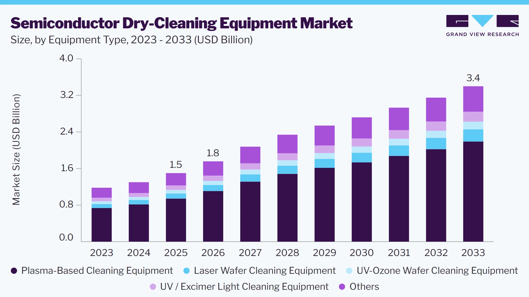
The global semiconductor dry cleaning equipment market size was valued at USD 1.5 billion in 2025 and is projected to grow from USD 1.8 billion in 2026 to USD 3.4 billion by 2033, at a CAGR of 9.9% from 2026 to 2033. Asia pacific dominated the global market with the largest revenue share of 86.6% in 2025. The market is driven by miniaturization of semiconductor devices, increasing process complexity, and stringent contamination control requirements. The global market is driven by the increasing complexity of semiconductor architectures, including 3D NAND, gate-all-around (GAA) transistors, and advanced packaging structures. These technologies require precise contaminant removal from increasingly delicate surfaces while preserving material integrity and device performance.
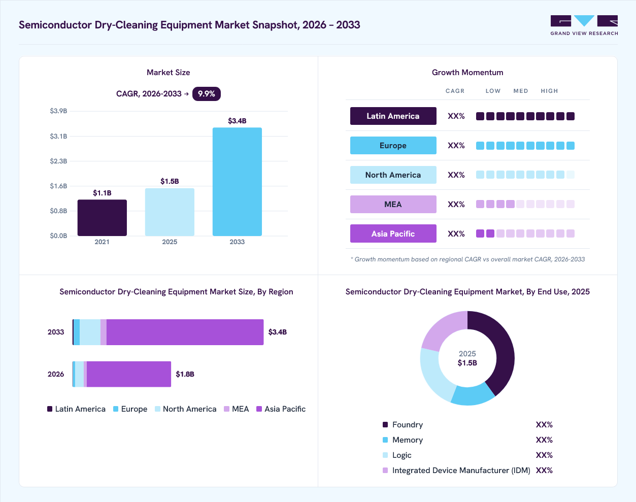 Source: Grand View Research, IR Documents, Primary Interviews, Paid DatabasesTo learn more about this report,
 Download Free Sample Report
Key Market Trends & Insights
- By equipment type: Plasma-based cleaning equipment segment dominated the market in 2025, holding 62.8% market share.
- By end use: Logic segment is projected to grow at a CAGR of 9.9% during the forecast period.
Regional Highlights
- Largest regional market: Asia pacific (86.6% revenue share, 2025)
- By country: Taiwan held the largest share of the Asia Pacific in 2025.
Market Size & Forecast
- Market Size in 2025: USD 1.5 Billion
- Estimated market size in 2026: USD 1.8 Billion
- Projected Market Size by 2033: USD 3.4 Billion
- CAGR (2026-2033): 9.9%
Prism AI by Grand View Research Free to tryAsk a question about the semiconductor dry cleaning equipment marketTry asking✓Every figure cited from GVR research Prefer the report? Download free sample →Investments in advanced wafer fabrication, high-bandwidth memory production, and semiconductor packaging infrastructure are generating additional demand for application-specific dry-cleaning equipment. Equipment procurement is increasingly shaped by contaminant profiles, substrate sensitivity, surface-cleanliness specifications, throughput requirements, and integration with existing fabrication processes, encouraging manufacturers to refine system capabilities in accordance with evolving semiconductor manufacturing requirements.
 To learn more about this report, Download Free Sample Report
Market Dynamics
The global semiconductor dry cleaning equipment market is shaped by the need for precise contaminant removal and controlled wafer surface preparation across semiconductor fabrication processes. Increasingly stringent cleanliness specifications, complex device structures, and sensitivity to surface defects are reinforcing the relevance of dry-cleaning technologies in removing organic residues, photoresist remnants, and other process-related contaminants. Market demand is influenced by semiconductor fabrication capacity, cleaning performance requirements, compatibility with advanced materials, and the ability to maintain wafer integrity without introducing undesirable surface modifications.
The progressive miniaturization of semiconductor devices and increasing complexity of logic and memory fabrication are intensifying requirements for controlled residue removal at critical manufacturing stages. Organic contaminants and process residues can interfere with subsequent operations, including thin-film deposition, surface conditioning, and wafer bonding, making effective cleaning essential to maintaining process consistency. Laser-based, UV-ozone, UV/excimer, and plasma-based technologies address specific contamination-removal requirements through mechanisms that can reduce dependence on liquid cleaning agents in suitable applications.
The adoption of semiconductor dry-cleaning equipment is constrained by stringent process qualification requirements and the need to balance contaminant removal with substrate preservation. Cleaning parameters must be carefully controlled to prevent surface damage, undesirable chemical modification, or inconsistencies across treated wafers. Differences in residue composition, material properties, and process conditions can necessitate application-specific optimization and extensive validation before equipment is incorporated into production lines.
The development of advanced semiconductor architectures and increasingly complex wafer-processing sequences creates opportunities for dry-cleaning equipment manufacturers. Precise surface preparation is becoming increasingly relevant in applications involving multilayer structures, dissimilar materials, and bonding interfaces, where residual contamination can compromise subsequent process steps. Advanced packaging, hybrid bonding, and three-dimensional integration provide additional avenues for specialized cleaning technologies, particularly where conventional cleaning approaches face material-compatibility or process-control limitations.
Market Concentration & Characteristics
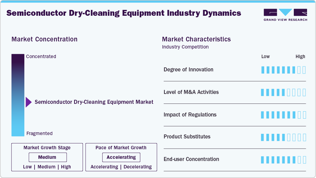
The semiconductor dry cleaning equipment market is moderately fragmented, comprising established semiconductor equipment manufacturers and specialized technology providers competing across laser-based, UV-ozone, UV/excimer, and plasma-based cleaning systems. Market fragmentation reflects the diversity of cleaning technologies, application-specific process requirements, and varying levels of technological specialization. Established suppliers benefit from extensive process expertise, customer qualification experience, and integration capabilities, while niche manufacturers differentiate themselves through specialized solutions for wafer surface preparation and contamination removal.
 To learn more about this report, Download Free Sample Report
The degree of innovation is closely linked to advances in semiconductor architectures, including 3D NAND, gate-all-around transistors, high-bandwidth memory, and hybrid bonding. Equipment development emphasizes precise residue removal, process selectivity, treatment uniformity, and compatibility with sensitive materials and interfaces. Manufacturers are refining process controls and cleaning configurations to minimize substrate damage and address increasingly stringent surface-preparation requirements across advanced fabrication and packaging applications.
Merger and acquisition activity is shaped by opportunities to expand technology portfolios, acquire specialized process expertise, and strengthen relationships with semiconductor manufacturers. Potential transactions may involve developers of specialized cleaning technologies, surface-treatment equipment, or complementary process-control solutions. Such strategic moves can broaden application coverage and facilitate entry into emerging semiconductor processes. However, transaction opportunities depend on technology compatibility, customer qualification requirements, and the strategic priorities of equipment manufacturers seeking to strengthen their market positions.
Analyst Perspective
The global semiconductor dry cleaning equipment market is evolving alongside advances in wafer fabrication, device miniaturization, and heterogeneous integration. Increasing process complexity and stringent surface-purity specifications are strengthening the requirement for cleaning technologies that remove residual contaminants without compromising substrate integrity or sensitive material interfaces. Plasma-based, laser, UV-ozone, and UV / excimer systems serve distinct process requirements, with their adoption determined by contaminant characteristics, material compatibility, and fabrication specifications. Continued investment in foundry infrastructure, memory production, and advanced packaging is expected to create procurement opportunities across established and emerging manufacturing facilities.
Equipment Type Insights
The plasma-based cleaning equipment segment dominated the global semiconductor dry cleaning equipment market in 2025, reflecting its established role in removing organic residues, photoresist remnants, and surface contaminants during wafer fabrication. Its adoption is supported by process versatility and compatibility with multiple semiconductor manufacturing stages, where effective contamination control is essential to maintaining wafer quality and process consistency. The technology remains relevant across logic and memory fabrication, particularly in applications requiring controlled surface treatment.
The laser wafer cleaning equipment segment is projected to register a CAGR of 10.6% during the forecast period. Growth is attributable to increasing demand for localized, high-precision contaminant removal across advanced semiconductor manufacturing processes. Laser-based systems offer opportunities for selective surface treatment with limited chemical consumption in suitable applications, making them relevant to processes involving sensitive materials and increasingly complex device structures. Continued advances in laser processing are expected to expand their applicability across specialized wafer-cleaning requirements.
End Use Insights
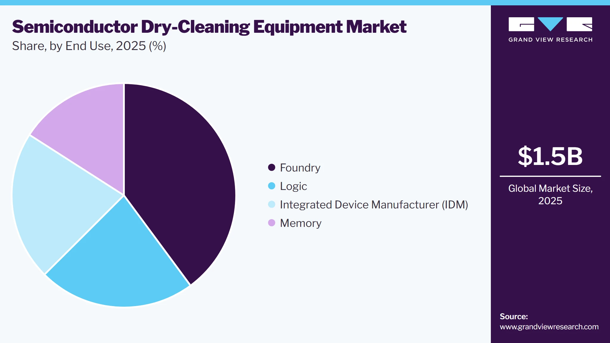
The foundry segment accounted for 39.9% of the global semiconductor dry cleaning equipment market in 2025, representing the largest share among end-use segments. Foundries manufacture semiconductor devices for a broad customer base, encompassing multiple technology nodes and product categories, which creates varied requirements for wafer cleaning and contamination control. Investments in fabrication capacity and the adoption of advanced process technologies continue to underpin demand for cleaning equipment across foundry manufacturing operations.
 To learn more about this report, Download Free Sample Report
The logic segment is projected to grow at a CAGR of 9.9% during the forecast period, supported by increasing process complexity in advanced logic device fabrication. The transition toward smaller feature dimensions and more intricate transistor architectures intensifies the need for precise residue removal and surface preparation at critical manufacturing stages. These requirements are reinforcing demand for dry-cleaning technologies capable of maintaining substrate integrity and meeting stringent process specifications.
Regional Insights
North America Semiconductor Dry Cleaning Equipment Market Trends
The North America semiconductor dry cleaning equipment market is projected to register a CAGR of 13.6% during the forecast period, supported by efforts to strengthen semiconductor manufacturing capabilities, expand advanced fabrication capacity, and improve supply-chain resilience. Investments in new semiconductor facilities, advanced packaging, and specialized manufacturing technologies are increasing demand for precise wafer-surface preparation and contamination control. The expansion of advanced logic and memory production, particularly in the U.S., is further supporting the adoption of plasma-based cleaning, laser wafer cleaning, UV-ozone cleaning, and UV/excimer cleaning equipment according to specific process requirements.
The U.S. semiconductor dry cleaning equipment market is upheld by domestic semiconductor manufacturing investments, increasing demand for advanced memory and logic chips, and efforts to strengthen the domestic semiconductor supply chain. Moreover, federal incentives under the CHIPS and Science Act have supported investments across advanced packaging, wafer fabrication, and semiconductor-related equipment and materials manufacturing. These investments are expanding the potential installed base of semiconductor manufacturing facilities, creating opportunities for dry-cleaning technologies used to remove organic contaminants, photoresist residues, and other surface impurities from wafers without conventional wet chemical processing.
Canada semiconductor dry cleaning equipment market is influenced by investments in specialized semiconductor manufacturing, advanced packaging, and photonics fabrication rather than a manufacturing base dominated by large-scale conventional silicon wafer foundries. Recent government initiatives are aimed at expanding domestic semiconductor production capabilities and strengthening Canada's position in specialized, high-value segments of the semiconductor supply chain. This creates opportunities for dry-cleaning equipment used in wafer fabrication and related manufacturing processes, although the scale of demand will depend on the equipment requirements of individual facilities.
Europe Semiconductor Dry Cleaning Equipment Market Trends
Europe's semiconductor dry cleaning equipment market is supported by its established semiconductor manufacturing ecosystem, advanced microelectronics research capabilities, and continued investment in specialized fabrication technologies. Regional demand is associated with wafer fabrication, power semiconductor production, sensor manufacturing, and advanced packaging, where stringent surface-cleanliness requirements necessitate precise contaminant removal. Equipment adoption is increasingly influenced by process compatibility, treatment uniformity, substrate integrity, operational reliability, and integration with existing semiconductor production lines.
Germany's semiconductor dry cleaning equipment market is supported by investments in domestic wafer-fabrication capacity, automotive semiconductor production, and advanced microelectronics manufacturing. The country's established automotive and industrial electronics industries generate demand for semiconductor devices with stringent performance and reliability requirements. Continued development of fabrication facilities and specialized semiconductor processes is strengthening the need for effective wafer-surface preparation and residue removal, creating opportunities for plasma-based, laser-based, UV-ozone, and UV/excimer cleaning technologies.
France's semiconductor dry cleaning equipment market is supported by initiatives to strengthen domestic semiconductor manufacturing, advance technological capabilities, and expand production of specialized microelectronic components. The country's focus on power semiconductors, energy-efficient electronics, sensors, and advanced chip technologies is reinforcing investment in fabrication processes requiring precise contamination control. As semiconductor manufacturing capabilities expand, demand for dry-cleaning equipment is expected to benefit from the need for controlled surface treatment, material compatibility, and consistent wafer preparation across specialized production applications.
Asia Pacific Semiconductor Dry Cleaning Equipment Market Trends
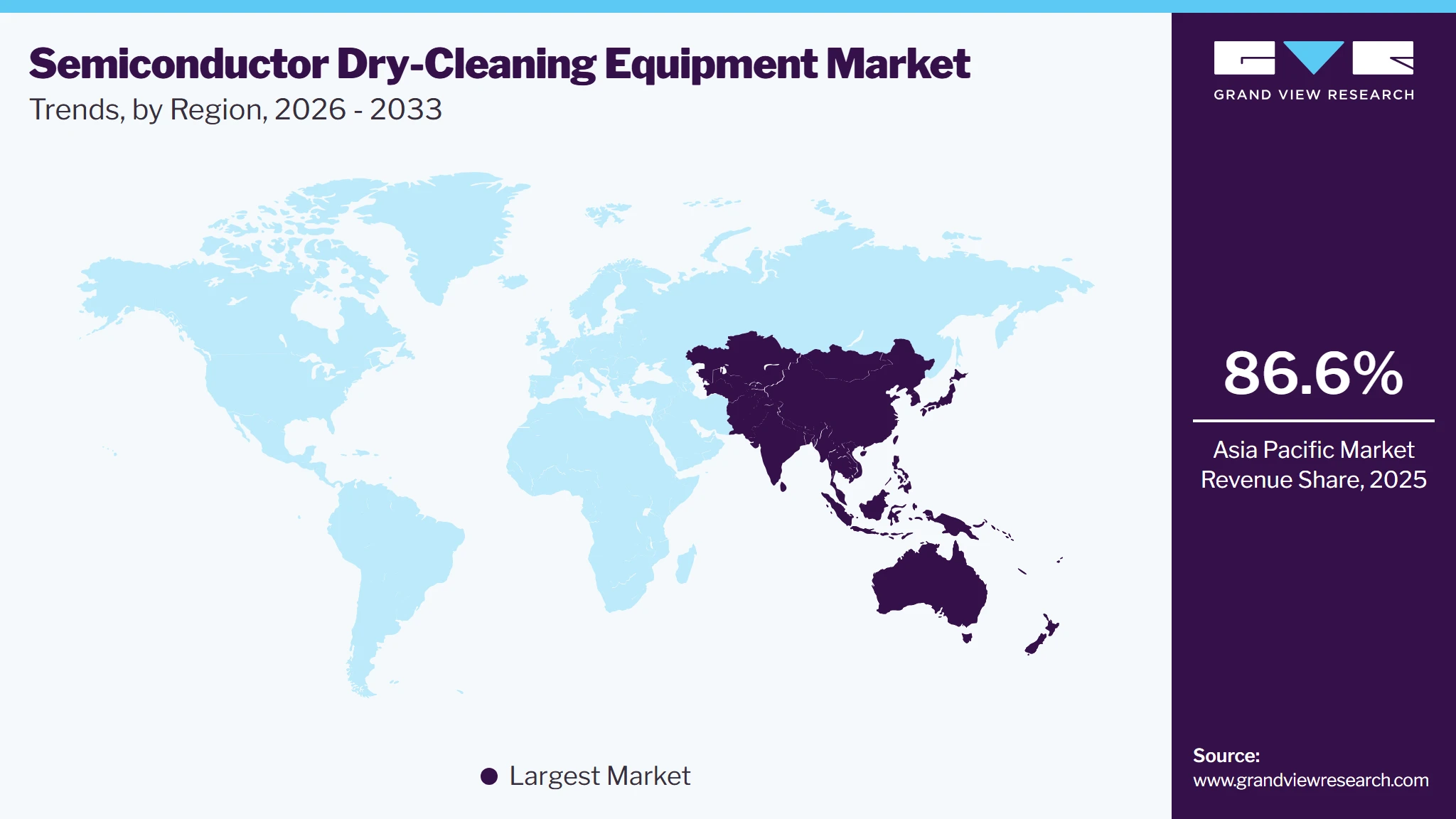
Asia pacific dominated the global market with the largest revenue share of 86.6% in 2025. The Asia Pacific semiconductor dry cleaning equipment market is followed by the region’s strong semiconductor manufacturing base, continued investment in advanced fabrication technologies, and efforts to strengthen domestic supply chains. China is expanding domestic wafer-fabrication capacity and developing local semiconductor equipment capabilities, while Taiwan continues to advance leading-edge logic manufacturing and advanced packaging. South Korea’s established memory-chip industry and investments in artificial intelligence-related semiconductors further support regional manufacturing activity.
 To learn more about this report, Download Free Sample Report
China’s semiconductor dry cleaning equipment market is supported by ongoing investments in domestic wafer-fabrication capacity, technological advancement in semiconductor manufacturing, and initiatives to strengthen indigenous equipment production. The expansion of logic and memory fabrication, alongside continued efforts to reduce reliance on imported semiconductor manufacturing technologies, is reinforcing demand for specialized wafer-cleaning solutions. Increasing emphasis on process precision, contamination control, and equipment localization is creating opportunities for domestic suppliers to develop dry-cleaning systems suited to evolving fabrication requirements.
India’s semiconductor dry cleaning equipment market is expected to benefit from the expansion of domestic semiconductor manufacturing and the government’s efforts to establish a more comprehensive semiconductor value chain. Under India Semiconductor Mission 2.0, announced in the Union Budget 2026 - 27, the government is prioritizing domestic semiconductor equipment and materials manufacturing, indigenous semiconductor intellectual property development, and industry-led research and training.
Taiwan held the largest share of the Asia Pacific semiconductor dry cleaning equipment market, accounting for 34.6% in 2025, attributable to its entrenched foundry ecosystem, concentration of advanced-node fabrication facilities, and technological leadership in wafer processing. Investments in 2-nm manufacturing, high-performance computing chips, and advanced packaging are intensifying requirements for precision-driven surface conditioning and residue elimination. The increasing intricacy of wafer architectures and interconnect structures is further elevating the importance of non-liquid contamination-removal processes, creating opportunities for plasma-based, UV-based, and laser-based cleaning equipment across advanced fabrication facilities.
Middle East & Africa Semiconductor Dry Cleaning Equipment Market Trends
The Middle East and Africa semiconductor dry cleaning equipment market is characterized by a limited base of commercial wafer fabrication facilities and emerging investment in semiconductor research and specialized manufacturing. Saudi Arabia is developing domestic capabilities through its National Capability Center for Semiconductors, which connects cleanroom facilities at King Abdulaziz City for Science and Technology (KACST) and King Abdullah University of Science and Technology (KAUST). The network provides access to more than 3,600 square meters of cleanroom facilities for semiconductor research, chip development, and practical training.
Israel’s semiconductor dry cleaning equipment market is supported by its established semiconductor fabrication base and continued investment in advanced chip technologies. Intel operates a major manufacturing facility in Kiryat Gat, while Tower Semiconductor specializes in silicon-germanium, silicon photonics, radio-frequency, mixed-signal, and power semiconductor technologies. In June 2026, the Israel Innovation Authority, in collaboration with the Directorate of Defense Research & Development at the Ministry of Defense, launched an initiative worth up to NIS 150 million (~ USD 51.4 million) to establish research and development infrastructure for next-generation integrated photonic chips.
Latin America Semiconductor Dry Cleaning Equipment Market Trends
The Latin America semiconductor dry cleaning equipment market is projected to register the fastest growth, with a CAGR of 14.6% during the forecast period, supported by efforts to strengthen domestic semiconductor capabilities, attract technology investment, and improve regional supply-chain resilience. Brazil is advancing local semiconductor production through government incentives and private-sector investment, while other countries are exploring opportunities in chip design, specialized electronics, assembly, testing, and packaging. These developments, alongside demand from automotive, telecommunications, and industrial applications, are creating opportunities for semiconductor dry-cleaning equipment across emerging regional manufacturing ecosystems.
Brazil’s semiconductor dry cleaning equipment market is supported by government initiatives and private-sector investment aimed at strengthening domestic semiconductor manufacturing and reducing reliance on imported components. The Support Programme for the Technological Development of the Semiconductor Industry (PADIS) provides fiscal incentives for eligible semiconductor activities, while the Brasil Semicon programme supports the development of the broader semiconductor value chain. Private-sector investment is also contributing to this expansion.
Key Semiconductor Dry Cleaning Equipment Company Insights
Some of the key players operating in the market include IMT Co., Ltd, JEOL Ltd., UVFAB Systems, Inc., among others.
-
IMT Co., Ltd. is a South Korea-based manufacturer specializing in dry-cleaning equipment for semiconductor and advanced IT manufacturing. The company has over 20 years of experience developing laser- and CO₂-based cleaning technologies that remove particles, residues, and other contaminants without using water or chemical cleaning agents. Its product portfolio includes high-bandwidth memory (HBM) wafer cleaning systems, semiconductor probe card and test socket cleaners, and equipment for removing molding residues and contaminants from semiconductor process components.
-
JEOL Ltd. has built its expertise in scientific instrumentation, electron optics, and precision engineering. Its product portfolio spans electron microscopes, analytical instruments, semiconductor manufacturing systems, industrial equipment, and medical devices. In the semiconductor sector, the company supplies electron beam lithography and inspection technologies, along with the SB-89010EUVC excimer UV cleaner, which removes organic contaminants from wafer surfaces before subsequent processing.
Key Semiconductor Dry Cleaning Equipment Companies
The following key companies have been profiled for this study on the semiconductor dry cleaning equipment market.
-
IMT Co., Ltd
-
JEOL Ltd.
-
UVFAB Systems, Inc.
-
Hamamatsu Photonics K.K.
-
Samco Inc.
-
Novascan Technologies, Inc.
-
LAM RESEARCH CORPORATION
-
Nordson Corporation
-
Oxford Instruments
-
PSK Inc.
-
COWINDST
-
ULVAC GmbH
-
Tokyo Electron Limited.
-
Bruker
-
PVA TePla AG
Competitive Benchmarking
Category
Operating Strategies
Competitive Edge
Weakness
Established Players (e.g., IMT Co., Ltd., JEOL Ltd., Hamamatsu Photonics K.K., Samco Inc., Nordson Corporation, Oxford Instruments)
Focus on developing specialized dry-cleaning systems and refining plasma, laser, ultraviolet, and cryogenic cleaning capabilities, according to individual product portfolios. Emphasize process selectivity, contamination removal, surface treatment, and integration with semiconductor fabrication and advanced packaging workflows.
Established engineering expertise, specialized cleaning technologies, and semiconductor industry relationships provide access to complex wafer-processing applications. Suppliers with dedicated dry-cleaning systems can differentiate through process control, substrate compatibility, and the ability to address stringent fabrication specifications.
High research and development expenditure, rigorous equipment qualification, and complex process integration can increase commercialization costs and extend customer adoption timelines. Exposure to semiconductor capital expenditure cycles may also contribute to fluctuations in equipment demand.
Emerging & Regional Players (e.g., UVFAB Systems, Inc., Novascan Technologies, Inc., and COWINDST)
Concentrate on specific cleaning methods, surface-treatment technologies, and application-defined equipment configurations, where these capabilities are established. Prioritize technical customization and targeted customer requirements rather than competing across the full spectrum of semiconductor manufacturing equipment.
Specialized technical capabilities and focused product development can address particular contamination-removal and surface-conditioning requirements. Targeted application expertise may provide differentiation in segments requiring specific cleaning methods or substrate-treatment characteristics.
Narrower product coverage, where applicable, may limit participation in procurement programs requiring multiple cleaning technologies or integrated process platforms. Customer qualification requirements, commercial reach, and the resources needed to validate equipment for semiconductor production can constrain broader market penetration.
Recent Developments
- In March 2026, Nordson Corporation expanded its agreement with Assembly Products, Inc., extending distribution and support for MARCH plasma systems across much of the U.S. and Canada. The expanded arrangement improves regional access to plasma equipment and customer support.
- In November 2025, Oxford Instruments and Quantemol announced a plasma-modelling R&D project supported by Innovate UK. The project combines plasma simulation with experimental validation on a PlasmaPro 100 Cobra ICP etching system to improve plasma-process precision and throughput.
Semiconductor Dry Cleaning Equipment Market Report Scope
Report Attribute
Details
Market size in 2025
USD 1.5 billion
Estimated market size in 2026
USD 1.8 billion
Projected market size by 2033
USD 3.4 billion
Growth Rate
CAGR of 9.9% from 2026 to 2033
Historical data
2021 - 2024
Forecast period
2026 - 2033
Quantitative units
Revenue in USD billion and CAGR from 2026 to 2033
Report coverage
Revenue forecast, company ranking, competitive landscape, growth factors, and trends
Segments covered
Equipment type, end use, region.
Regional scope
North America, Europe, Asia Pacific, Latin America, Middle East & Africa
Country scope
U.S.; Canada; Mexico; UK; Germany; France; Italy; Spain; Netherlands; China; Japan; India; Taiwan; South Korea; Brazil; Israel
Key companies profiled
IMT Co., Ltd; JEOL Ltd.; UVFAB Systems, Inc.; Hamamatsu Photonics K.K.; Samco Inc.; Novascan Technologies, Inc.; LAM RESEARCH CORPORATION; Nordson Corporation; Oxford Instruments; PSK Inc.; COWINDST; ULVAC GmbH; Tokyo Electron Limited.; Bruker; PVA TePla AG
Customization scope
Free report customization (equivalent up to 8 analysts working days) with purchase. Addition or alteration to country, regional & segment scope.
Pricing and purchase options
Avail customized purchase options to meet your exact research needs. Explore purchase options
Global Semiconductor Dry Cleaning Equipment Market Report Segmentation
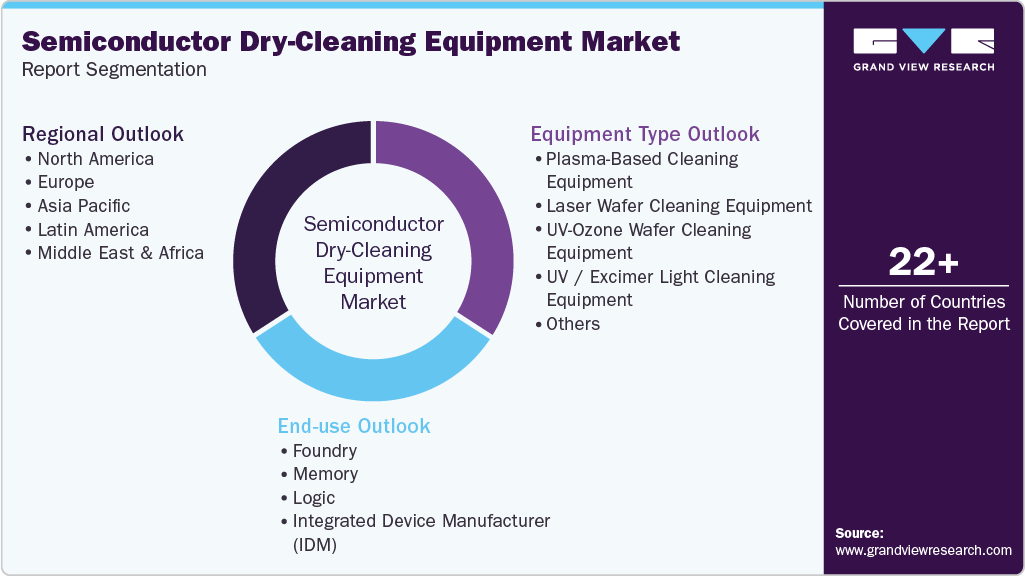
This report forecasts revenue growth at global, regional, and country levels and provides an analysis of the latest industry trends in each of the sub-segments from 2021 to 2033. For this study, Grand View Research has segmented the global semiconductor dry cleaning equipment market report based on equipment type, end use, and region.
 To learn more about this report, Download Free Sample Report
-
Equipment Type Outlook (Revenue, USD Billion, 2021 - 2033)
-
Plasma-Based Cleaning Equipment
-
Laser Wafer Cleaning Equipment
-
UV-Ozone Wafer Cleaning Equipment
-
UV / Excimer Light Cleaning Equipment
-
Others
-
-
End Use Outlook (Revenue, USD Billion, 2021 - 2033)
-
Foundry
-
Memory
-
Logic
-
Integrated Device Manufacturer (IDM)
-
-
Regional Outlook (Revenue, USD Billion, 2021 - 2033)
-
North America
-
U.S.
-
Canada
-
Mexico
-
-
Europe
-
Germany
-
Spain
-
France
-
Italy
-
UK
-
Netherlands
-
-
Asia Pacific
-
China
-
India
-
Japan
-
Taiwan
-
South Korea
-
-
Latin America
-
-
Brazil
-
-
Middle East and Africa
-
Israel
-
-
Research Methodology
The semiconductor dry cleaning equipment market figures in this report are based on a proven research process that combines executive interviews with secondary research from proprietary databases, company filings, and recognized regulatory and institutional sources. Market size is built through value-chain sizing-reconciling supply-side and demand-side estimates-and triangulated with bottom-up and top-down approaches. Every estimate passes multiple levels of expert validation before publication, with each semiconductor dry cleaning equipment segment quantified using the revenue-capture definitions in the table below.
Segment Definition
Equipment Type
Revenue Capture Definition
Plasma-Based Cleaning Equipment
Revenue generated from the sale of plasma-based cleaning equipment that removes photoresist residues, organic contaminants, and surface impurities from semiconductor wafers through plasma-assisted processes.
Laser Wafer Cleaning Equipment
Revenue generated from the sale of laser wafer cleaning equipment that eliminates particles, residual materials, and surface contaminants from semiconductor wafers using laser-based cleaning processes.
UV-Ozone Wafer Cleaning Equipment
Revenue generated from the sale of UV-ozone wafer cleaning equipment that decomposes organic contaminants and surface residues through ultraviolet irradiation and ozone-induced oxidation.
UV / Excimer Light Cleaning Equipment
Revenue generated from the sale of UV and excimer light cleaning equipment that removes organic residues and contaminants through short-wavelength ultraviolet radiation and photochemical reactions.
Others
Revenue generated from the sale of other semiconductor dry-cleaning equipment, including cryogenic, carbon dioxide (CO₂)-based, and vapor-phase cleaning systems designed to remove contaminants from semiconductor wafers and related surfaces.
End Use
Revenue Capture Definition
Foundry
Revenue generated from the sale of semiconductor dry-cleaning equipment to foundries engaged in contract wafer fabrication for fabless companies and other semiconductor customers.
Memory
Revenue generated from the sale of semiconductor dry-cleaning equipment to manufacturers of memory devices, including DRAM and NAND flash, for contamination control during wafer fabrication.
Logic
Revenue generated from the sale of semiconductor dry-cleaning equipment to manufacturers of logic devices, including processors, controllers, and application-specific integrated circuits, for contamination management across wafer fabrication processes.
Integrated Device Manufacturer (IDM)
Revenue generated from the sale of semiconductor dry-cleaning equipment to integrated device manufacturers that combine semiconductor design and fabrication within their operations and may also undertake assembly and testing.
Estimation Model
Layer Name
Key Question
Description
Demand Assessment Layer
What establishes the underlying demand for semiconductor dry-cleaning equipment?
Evaluate semiconductor manufacturing activity across foundries, memory producers, logic device manufacturers, and integrated device manufacturers (IDMs). Examine wafer fabrication volumes, process-node miniaturization, contamination-control requirements, and advanced packaging adoption to establish the underlying demand for dry-cleaning solutions across semiconductor manufacturing operations.
Capital Investment & Procurement Layer
Which investment patterns translate into equipment procurement?
Analyze capital expenditure on new fabrication facilities, wafer production capacity additions, and technology upgrades. Assess fab construction timelines, manufacturing expansion plans, equipment replacement cycles, and procurement priorities to determine how semiconductor industry investments translate into demand for dry-cleaning equipment.
Equipment Type & Application Assessment Layer
How are dry-cleaning technologies allocated across semiconductor manufacturing applications?
Assess the applicability of plasma-based, laser wafer, UV-ozone, UV / excimer light, and other dry-cleaning technologies across wafer fabrication and related processing stages. Evaluate technology selection according to contaminant characteristics, substrate compatibility, surface sensitivity, process requirements, and cleaning precision to establish the suitability of individual equipment categories for specific manufacturing applications.
Market Revenue Estimation Layer
How is annual market revenue quantified?
Quantify annual market revenue by equipment type, end-use category, and geographic market using equipment sales volumes and realized selling prices. Incorporate demand from new installations, production-line additions, and replacement purchases, while accounting for variations in equipment configuration, technological complexity, automation, and system pricing.
Delivered Customizations
This report has been delivered with the following In-depth customizations
Client Request
Customization Delivered
Value Adds
Competitive Benchmarking
Evaluated leading semiconductor dry-cleaning equipment manufacturers based on product portfolio, cleaning technology expertise, process integration capabilities, engineering competencies, and geographic presence. The assessment covered plasma-based, laser wafer, UV-ozone, UV / excimer light, and other dry-cleaning technologies.
Provides a structured comparison of competitive positioning, technological capabilities, and product specialization. The findings facilitate competitor assessment, identification of capability gaps, and evaluation of opportunities for portfolio expansion and technological differentiation.
Regional Segmentation
Assessed North America, Europe, Asia Pacific, Latin America, and the Middle East & Africa based on semiconductor fabrication capacity, foundry and memory production, government support initiatives, manufacturing localization, and investments in semiconductor infrastructure.
Delineates regional differences in manufacturing activity, investment patterns, and equipment procurement potential. The analysis informs geographic prioritization, country-level market assessment, and strategic decisions concerning market entry and resource allocation.
Opportunity Assessment
Examined commercial prospects across equipment categories and end-use segments, including foundries, memory manufacturers, logic device producers, and integrated device manufacturers (IDMs). The evaluation considered advanced process-node development, high-bandwidth memory manufacturing, wafer bonding, heterogeneous integration, and the establishment and expansion of fabrication facilities.
Identifies attractive market segments and emerging commercial opportunities associated with evolving semiconductor manufacturing requirements. The findings support investment prioritization, assessment of technology-specific demand, and the formulation of targeted business development strategies.
About the Author(s)
Advanced Interior Materials Research Team
Advanced Materials · Advanced Interior MaterialsThis report was authored by the advanced interior materials research team at Grand View Research - comprising two research analysts, one senior research analyst, and one industry expert - with specialized expertise in the advanced interior materials segment of the advanced materials industry. All findings are based on proprietary advanced materials databases, executive interviews, and regulatory analysis, subject to internal peer review prior to publication.
Last Updated:
Speak to Analyst

Customize this report to your needs - add regions, segments, or data points, with 20% free customization.
Or view our licence options:


ISO 9001:2015 & 27001:2022 Certified
We are GDPR and CCPA compliant! Your transaction & personal information is safe and secure. For more details, please read our privacy policy.


