
- Home
- »
- Medical Devices
- »
-
Atomic Force Microscopy Market Size Report, 2026-2033GVR Report cover
![Atomic Force Microscopy Market (2026 - 2033)Report]()
Atomic Force Microscopy Market (2026 - 2033)
Size, Share & Trends Analysis Report By Application (Material Science, Semiconductors, Life Science, Nanotechnology, Other Applications), By Region, And Segment Forecasts
Market Size, 2025
$919.2MMarket Estimate, 2026
$993.0MMarket Forecast, 2033
$1,780.9MCAGR, 2026–2033
8.7%Atomic Force Microscopy Market Summary
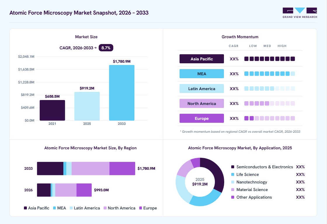
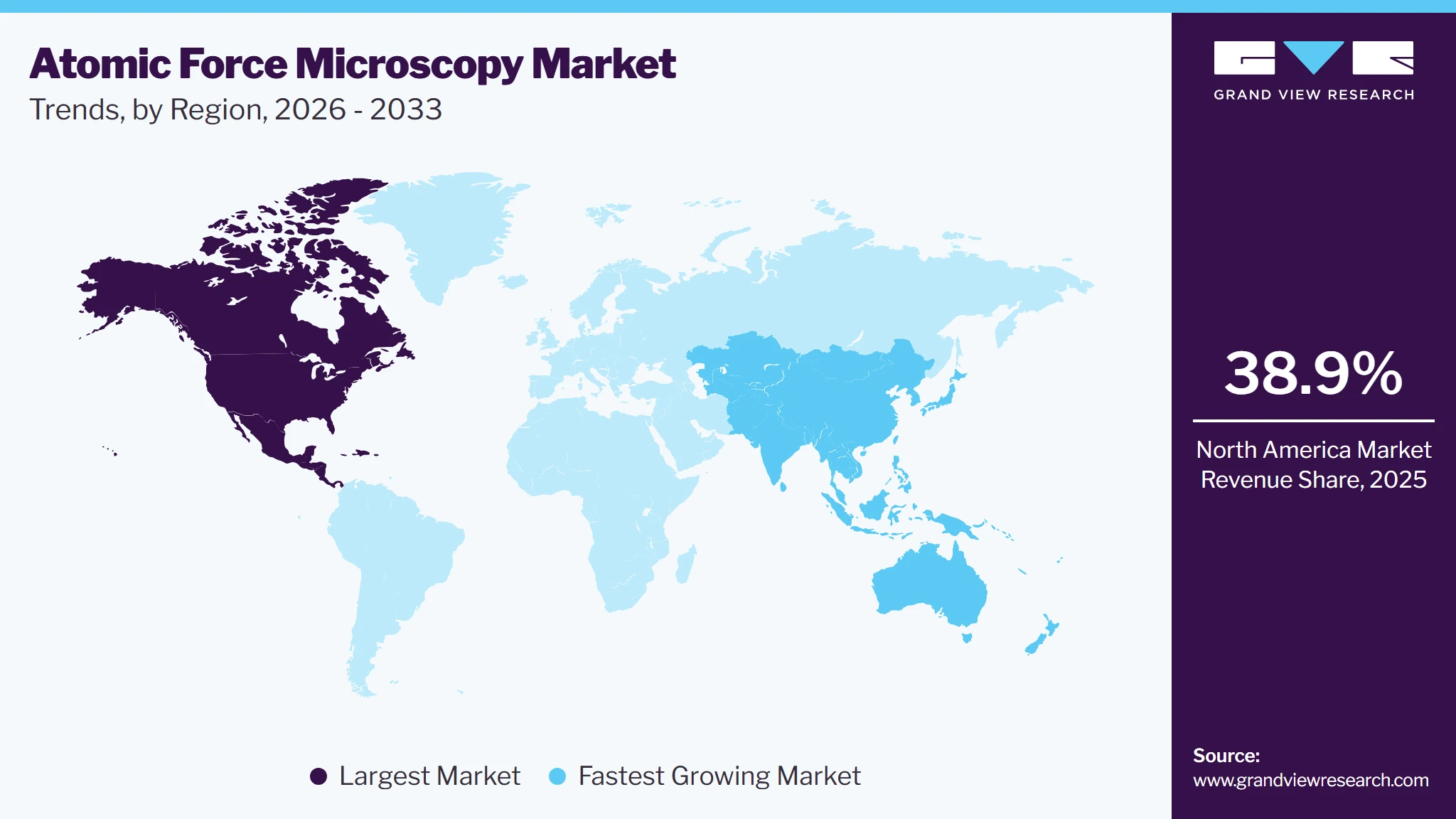
The global atomic force microscopy market size was valued at USD 919.2 million in 2025 and is projected to grow from USD 993.0 million in 2026 to USD 1,780.9 million by 2033, at a CAGR of 8.7% from 2026 to 2033. North America dominated the market, accounting for a revenue share of 38.9% in 2025. The market growth is attributed to the growing demand for high-resolution surface characterization and nanoscale imaging across materials science, semiconductors, life sciences, nanotechnology, and pharmaceuticals.
Key Market Trends & Insights
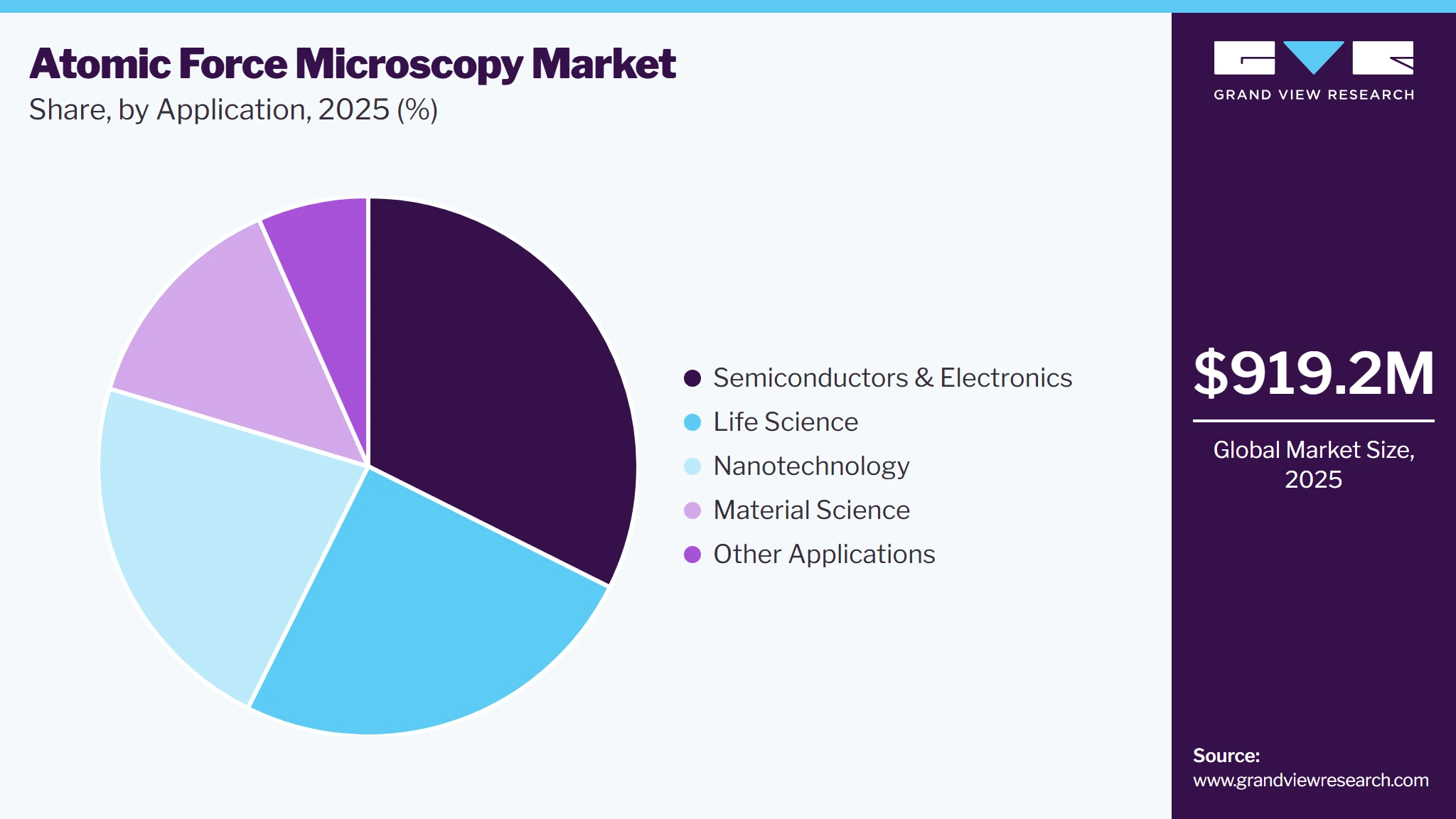
- By application: The semiconductors & electronics segment held the largest revenue share of 32.4% in 2025.
Regional Highlights
- Largest regional market: North America (38.9% revenue share, 2025)
- Fastest-growing regional market: Asia Pacific (highest CAGR, 2026-2033)
- By country: The U.S. held the largest market share in 2025
Market Size & Forecast
- Market size in 2025: USD 919.2 Million
- Estimated market size in 2026: USD 993.0 Million
- Projected market size by 2033: USD 1,780.9 Million
- CAGR (2026-2033): 8.7%
The rapid growth of nanotechnology and advanced materials research is further increasing the need for precise characterization tools, while continued miniaturization in the semiconductor and electronics industries is driving demand for nanoscale inspection and defect analysis. In addition, expanding biomedical and pharmaceutical research including cell, protein, DNA, biomaterial, and drug-delivery studies is creating new applications for AFM.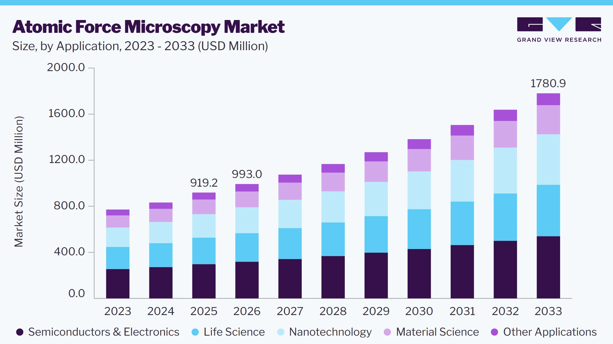
Market Dynamics
The section below outlines the key factors driving the growth of the atomic force microscopy market, highlighting the increasing demand for high-resolution nanoscale imaging and characterization across life sciences, materials science, and semiconductor research. It also examines the growing adoption of AFM for nanotechnology and surface analysis, rising investments in semiconductor and advanced materials development, technological advancements such as high-speed and multimodal AFM, expanding applications in biological and pharmaceutical research, and increasing demand for precise nanoscale characterization in academic, industrial, and research laboratories.
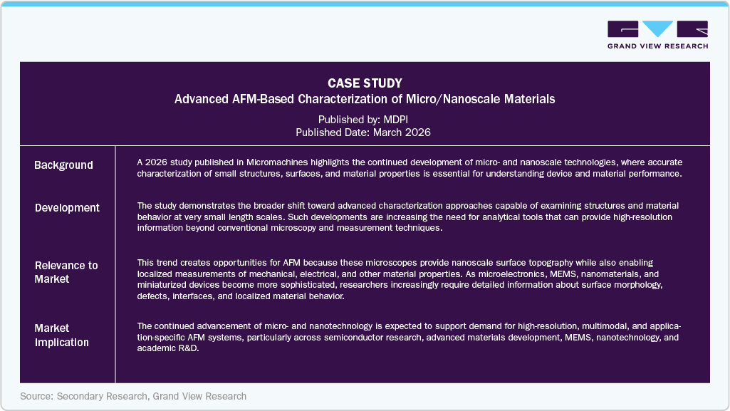
As research and industrial development increasingly shift toward nanometer-scale materials, devices, and structures, conventional optical microscopy often cannot provide sufficient resolution or detailed information about surface properties. AFM addresses this need by enabling three-dimensional surface imaging at the nanoscale while also allowing researchers to measure properties such as roughness, adhesion, elasticity, friction, electrical potential, conductivity, and mechanical response. This multifunctionality is particularly important for advanced materials, where performance is strongly influenced by surface and interfacial characteristics. Reviews of AFM applications in nanomaterials and 2D materials have highlighted its ability to provide topographical information and mechanical, electrical, optical, chemical, and electrochemical measurements.
Argonne National Laboratory’s development of DONUT (Data Optimization and Navigation Utility Tool) in August 2026 demonstrates the growing importance of real-time, data-driven characterization in advanced materials research. The initiative uses automated data analysis to process high-volume X-ray measurements generated during experiments at Argonne’s Advanced Photon Source, enabling researchers to interpret experimental results much faster instead of waiting for extensive post-processing. This is significant for materials science because modern synchrotron experiments can generate very large datasets while researchers investigate material structures and behavior under changing conditions. Faster analysis allows scientists to identify meaningful results during experiments, adjust experimental parameters, and accelerate the overall materials discovery cycle.
The expanding application of AFM across life sciences, biotechnology, pharmaceutical research, semiconductors, and electronics is a major driver of the market, as researchers and manufacturers increasingly require high-resolution characterization of surfaces, structures, mechanical properties, and molecular interactions at the nanoscale. In life sciences and biotechnology, AFM enables researchers to visualize cells, proteins, DNA, membranes, viruses, and other biological structures under near-physiological conditions while also measuring properties such as cell stiffness, adhesion, surface roughness, and molecular forces.
The use of AFM is also expanding in pharmaceutical and drug-development research, particularly for characterizing nanoparticles, drug-delivery systems, proteins, and drug-cell interactions. AFM provides both morphological and nanomechanical information, allowing researchers to examine nanoparticle size, surface properties, stability, adhesion, and interactions with biological membranes. A 2025 Materials Today Bio review highlighted applications ranging from characterization of soft nanoparticles for drug delivery to measurement of antibody-antigen and ligand-receptor binding forces. This creates opportunities for AFM adoption in biologics development, nanomedicine, vaccine research, formulation development, and targeted drug-delivery studies.
Recent technological developments are further strengthening the biological and pharmaceutical use case. High-speed AFM (HS-AFM) has improved the ability to observe biological structures in real time rather than relying only on static images. For instance, a February 2026 ACS Nano review described HS-AFM as an important tool for real-time nanoimaging of disease-relevant structures under near-physiological conditions, including research related to infectious diseases, cancer, infertility, and neurodegeneration. In another February 2026 study published by National Library of Medicine, live-cell AFM was used to characterize membrane-protein dynamics and distinguish cell types based on nanoscale surface characteristics, demonstrating potential applications in cancer research, neuroscience, and drug development.
Recent Development
ORNL Develops Large-Area AFM for High-Throughput Biofilm Imaging
Background
In August 2025, researchers at the U.S. Department of Energy’s Oak Ridge National Laboratory (ORNL) developed an automated large-area atomic force microscopy (AFM) platform to overcome a major limitation of conventional AFM-its relatively narrow field of view. The technology was demonstrated on bacterial biofilms, enabling researchers to examine individual bacterial cells while also capturing their organization across much larger surface areas.
Technology Development
The key advancement was the integration of automated AFM imaging with machine learning. The system generated large-area, high-resolution images and automatically analyzed more than 19,000 individual bacterial cells, allowing researchers to quantify cell properties and identify large-scale organizational patterns. The study revealed honeycomb-like bacterial arrangements interconnected by flagella, providing insights into how biofilms form and maintain their structure.
Application
The researchers also used the platform to evaluate engineered surfaces containing nanoscale ridges. Certain surface patterns were found to disrupt normal biofilm formation, highlighting the potential of AFM-based characterization for developing antifouling surfaces for applications in healthcare, food safety, industrial equipment, and water systems.
Relevance to Market
The development demonstrates how AFM is evolving beyond conventional small-area nanoscale imaging toward large-area, automated, high-throughput, and data-driven characterization. The integration of machine learning increases the ability to process large datasets and extract quantitative insights, expanding AFM applications in life sciences, microbiology, biomaterials, and surface engineering.
Market Implication
The ORNL development highlights an important growth opportunity for AFM manufacturers to offer automated large-area imaging, AI/ML-enabled analysis, and high-throughput characterization capabilities. Such advancements can expand the addressable market by making AFM more suitable for complex biological and materials applications where researchers need to connect nanoscale features with larger-scale structural behavior.
Source: Oak Ridge National Laboratory, Secondary Research, Grand View Research
The high acquisition cost and technical complexity of Atomic Force Microscopy (AFM) systems represent a significant restraint to market adoption, particularly for small and medium-sized laboratories, academic institutions, startups, and research organizations with limited capital budgets. AFM systems typically require substantial investment in the core microscope and in specialized scanners, probes, vibration-isolation equipment, software, installation, training, and maintenance. According to the provided AFMWorkshop pricing information, general-purpose AFM systems can range from approximately USD 20,000 to USD 300,000, depending on imaging resolution, automation, scanning range, and specialized capabilities. Basic systems priced below USD 30,000 generally offer limited modes and lower specifications, whereas advanced systems exceeding USD 100,000 incorporate features such as motorized sample positioning, automated focusing, very low noise floors, and advanced measurement capabilities. This wide price range creates a substantial entry barrier for institutions that require AFM only for occasional or basic characterization.
AFM Price Range
Typical Characteristics
Typical Users / Applications
USD 20,000-30,000
Basic AFM, cell-phone-type optics, noise floor >250 pm, limited operating modes
Education, student training, basic imaging
USD 30,000-100,000
Tabletop, high-resolution, life-science, nano-profiling and standalone systems
Academic and industrial researchers requiring routine AFM imaging
USD 100,000-300,000
Motorized sample stage, automated focus, noise floor <50 pm, advanced software and specialized modes
AFM experts, advanced materials, semiconductors and life-science research
Source: AFM Workshop, USA, Secondary Research, Grand View Reseearch
The AFM Workshop price list further demonstrates that the total cost of ownership extends well beyond the microscope itself. For instance, TT-2 systems are priced at approximately USD 41,587-84,357, while high-resolution AFM systems range from USD 49,977-94,091. Specialized systems such as HR-2D AFM for two-dimensional materials range from USD 42,215-56,634, while NP/LS/SA systems can reach USD 107,555. Additional scanners can cost approximately USD 4,088-5,402, while installation and training can add USD 2,257-10,810. Specialized measurement modes, including conductive AFM, magnetic force microscopy, electric force microscopy, scanning Kelvin probe microscopy, and lithography, can add another USD 1,244-5,402. Consequently, laboratories seeking a fully equipped AFM platform can face considerably higher expenditure than the headline instrument price.
AFM Price Range
Typical Characteristics
Typical Users / Applications
TT-2 AFM
41,587-84,357
Core tabletop AFM investment
HR AFM
49,977-94,091
Higher-resolution imaging
HR-2D AFM
42,215-56,634
Specialized 2D-material characterization
B-3 AFM
37,831-42,179
Basic AFM platform
NP/LS/SA AFM
47,485-107,555
Nano-profiling and life-science applications
Scanners & options
4,088-5,402
Additional scanning capability
Installation & training
2,257-10,810
Setup, training and service
Specialized modes
1,244-5,402
C-AFM, MFM, EFM, SKPM, lithography, etc.
Accessories, components & probes
254-15,184
Consumables and additional hardware
Vibration solutions
1,244-10,792
Isolation cabinets/platforms
Repair & refurbishment
150-10,761
Ongoing maintenance and upgrades
Source: AFM Workshop, USA, Secondary Research, Grand View Research
The growing demand for customized and application-specific AFM systems represents a significant opportunity for market players, as research and industrial users increasingly require instruments optimized for specific materials, sample types, environments, and nanoscale properties rather than conventional general-purpose imaging. The expanding application base of AFM across semiconductors and microelectronics, 2D materials, thin films, energy storage, polymers, biomaterials, life sciences, and nanomechanical characterization is encouraging manufacturers to develop modular systems with specialized probes, stages, software, environmental controls, and measurement modes. Oxford Instruments, for instance, offers AFM configurations covering applications ranging from semiconductor and microelectronics research to graphene and 2D materials, biomolecules, cells and tissues, energy storage, photovoltaics, and nano-electrical characterization. This specialization enables manufacturers to address application-specific requirements such as electrical characterization for semiconductor devices, mechanical mapping for biomaterials, high-speed imaging for dynamic biological processes, and controlled-atmosphere or liquid-phase measurements for advanced materials research.
Another important opportunity is the development of specialized AFM platforms for advanced materials and emerging technologies. For 2D materials, for instance, AFMs increasingly need to characterize morphology and electrical, mechanical, and functional properties. Oxford Instruments has developed application-specific capabilities for materials such as graphene and MoS₂, including nanoscale electrical and functional measurements and operation under controlled environments.
Market Concentration & Characteristics
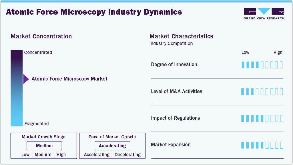
The chart below illustrates the relationship among industry concentration, industry characteristics, and key market participants in the market. The market is moderately consolidated, with a combination of established global microscopy manufacturers, specialized AFM technology providers, and research-instrument companies. Key participants compete through advanced imaging capabilities, high-resolution measurement technologies, application-specific solutions, software integration, and customized AFM systems for applications across semiconductors, materials science, life sciences, nanotechnology, and academic research.
The market is witnessing a high degree of innovation. Manufacturers are increasingly focusing on improving spatial resolution, imaging stability, measurement speed, and ease of operation to expand AFM applications across semiconductors, advanced materials, nanotechnology, and life sciences. For instance, in December 2024, Bruker introduced the Dimension Nexus Atomic Force Microscope, representing a significant product development aimed at making advanced AFM capabilities more accessible to growing laboratories and multi-user research facilities.
Dr. Alice Pyne, Head of the Henry Royce Nanocharacterisation Laboratory at the University of Sheffield. Said:
“I especially appreciate the compact and upgradable nature of the Dimension Nexus large-sample AFM, and the fact that it can perform the latest PeakForce Tapping modes. I can see this being a real advantage for multi-user labs, where AFM expertise and applications vary, and where physical space for instruments is at a premium.”
The level of M&A activities in the atomic force microscopy (AFM) market is moderate, with companies pursuing targeted acquisitions to expand technology portfolios, strengthen component capabilities, and support growth in semiconductor and advanced-material applications. For instance, in June 2026 Park Systems' acquisition of Rocky Mountain Nanotechnology (RMN) strengthened its AFM probe manufacturing capabilities and enabled greater vertical integration of critical AFM components. In addition, Park Systems has pursued acquisitions in complementary microscopy and nanometrology technologies, indicating a broader strategy of expanding its integrated characterization portfolio.
Karen Cho, Senior Executive Vice President at Park Systems said:
"As semiconductor process nodes shrink and advanced packaging architectures grow more complex, the need for sub-nanometer surface metrology has become critical across front-end and back-end semiconductor manufacturing. We believe this investment will strengthen our ability to meet growing customer demand and better serve customers worldwide."
The impact of regulations on the atomic force microscopy (AFM) market is moderate, as manufacturers must comply with electrical safety, electromagnetic compatibility, environmental, and laser-safety requirements across major markets. Regulations such as EU CE marking and RoHS influence product design, testing, documentation, and material selection, while laser-based AFM systems may require additional safety compliance. These requirements can increase development costs and time-to-market but also improve product safety, reliability, and quality, creating entry barriers for smaller manufacturers.
In May 2025, Oxford Instruments introduced the Jupiter Discovery AFM, representing a significant product development aimed at making high-performance AFM more accessible to both academic and industrial researchers. The system delivers a noise floor below 25 picometers and scan rates 5-20 times faster than other large-sample AFMs, improving resolution, throughput, and productivity. It also incorporates features such as pre-mounted probes, one-click laser alignment, automated imaging through AutoPilot, and intuitive operating software, reducing the expertise and training required for AFM operations.
Analyst Perspective
The atomic force microscopy market is witnessing steady growth, driven by increasing demand for high-resolution nanoscale characterization, growing nanotechnology research, and expanding applications across materials science, life sciences, and semiconductors & electronics. Rising semiconductor miniaturization, development of advanced materials and 2D materials, and increasing research into nanoscale surface properties are accelerating the adoption of advanced AFM systems globally. Ongoing advancements in high-speed AFM, multimodal imaging, automated measurement, AI-assisted analysis, and integrated AFM techniques such as AFM-Raman and nano-IR are enhancing measurement accuracy, workflow efficiency, and application capabilities, supporting the expansion of modern atomic force microscopy systems across both developed and emerging markets.
Application Insights
The semiconductors & electronics segment accounted for the largest market revenue share of 32.4% in 2025. The rapid miniaturization of semiconductor devices and increasing complexity of advanced chip architectures are driving demand for AFM as manufacturers require highly precise nanoscale characterization and process-control technologies.

AFM enables measurement of surface roughness, critical dimensions, trench and hole structures, thin films, nanoscale defects, and wafer topography, supporting process optimization and yield improvement. In addition, the expansion of AI-chip manufacturing is creating further demand for advanced semiconductor metrology; in June 2026, Nearfield Instruments raised USD 380 million to expand production and customer support for its AFM-based semiconductor metrology systems amid strong demand from advanced chipmakers.
The nanotechnology segment is expected to register the fastest CAGR over the forecast period due to the growing adoption of nanotechnology across electronics, advanced materials, energy, healthcare, and life sciences. AFM enables high-resolution measurement of surface morphology as well as mechanical, electrical, chemical, thermal, magnetic, and electrochemical properties, making it particularly valuable for nanomaterial development and characterization. The development of a microlens-augmented AFM platform by researchers at the Shenzhen Institutes of Advanced Technology, Chinese Academy of Sciences, reported in August 2025. The platform achieved more than a 10-fold improvement in imaging resolution, over 50% higher manipulation accuracy, and approximately 200% greater operational efficiency, while successfully tracking and manipulating 200-nm silver nanowires.
Regional Insights
North America Atomic Force Microscopy Market Trends
North America dominated the market with a revenue share of 38.9% in 2025, driven by strong semiconductor R&D, advanced materials research, biotechnology, and nanotechnology infrastructure, with increasing demand for high-resolution characterization and multimodal nanoscale analysis. AFM is increasingly used for semiconductor defect inspection, surface roughness, critical-dimension measurement, and electrical, mechanical, thermal, and chemical characterization. Bruker highlighted in 2025 that AFM has applications across semiconductor R&D, failure analysis, and high-volume manufacturing, supporting continued adoption in the region. The region is also benefiting from the growing integration of AFM with complementary techniques and automation, particularly for advanced semiconductor and materials applications.
U.S. Atomic Force Microscopy Market Trends
Atomic force microscopy market in the U.S.is supported by substantial university and government-funded nanotechnology research, semiconductor innovation, life-science research, and advanced materials development. The increasing complexity of semiconductor devices and demand for nanoscale failure analysis are expanding AFM applications beyond conventional surface imaging toward electrical, mechanical, thermal, and chemical characterization. Bruker's 2025 semiconductor AFM activities demonstrate the growing use of advanced AFM modes for device characterization and failure analysis. In addition, the U.S. focus on next-generation semiconductors, quantum technologies, and advanced materials is expected to sustain demand for sophisticated research-grade AFM platforms.
Europe Atomic Force Microscopy Market Trends
Europe's AFM market is benefiting from strong nanotechnology research, advanced materials development, semiconductor investments, and government initiatives to strengthen regional technology sovereignty. The European Chips Act has mobilized significant public and private investment toward semiconductor manufacturing and research, while the proposed Chips Act 2.0, announced in June 2026, aims to further strengthen advanced chip production and reduce strategic dependencies. These developments support demand for nanoscale metrology technologies such as AFM for wafer characterization, defect analysis, thin-film analysis, and advanced packaging research.
Germany atomic force microscopy market is anticipated to grow considerably during the forecast period due to its strong semiconductor, automotive electronics, industrial manufacturing, materials science, and research ecosystem. Increasing development of power semiconductors, sensors, photonics, and advanced materials is creating demand for nanoscale surface and material characterization. Germany's position within Europe's semiconductor ecosystem is further supported by the EU Chips Act, which is encouraging new semiconductor manufacturing and research capacity across member states. AFM therefore has opportunities in semiconductor R&D, quality control, failure analysis, thin-film characterization, and nanomechanical testing.
Atomic force microscopy market in the UK is driven primarily by strong academic R&D, compound semiconductor development, advanced materials research, quantum technologies, and semiconductor design. The UK's National Semiconductor Strategy specifically identifies compound semiconductors, R&D, advanced materials, photonics, quantum technologies, and heterogeneous integration as strategic areas, with up to USD 1.15 billion of investment planned over the next decade. These investments create opportunities for AFM systems in university laboratories, semiconductor R&D centers, advanced-materials development, and characterization of next-generation devices.
Asia Pacific Atomic Force Microscopy Market Trends
The Asia Pacific atomic force microscopy market is emerging as the fastest-growing region and is expected to remain one of the most dynamic AFM markets because of its large semiconductor manufacturing base, electronics industry, nanotechnology research, and advanced-materials development. Increasing semiconductor fabrication and packaging activities in China, South Korea, Japan, Taiwan, and emerging manufacturing hubs are generating demand for automated and high-throughput nanoscale metrology. Park Systems has expanded its industrial AFM portfolio specifically for semiconductor applications, including large-sample systems designed for 300-mm wafer analysis, reflecting the region's movement toward production-oriented AFM applications.
The China atomic force microscopy market is being supported by rapid development of semiconductors, electronics, nanomaterials, batteries, and advanced manufacturing, alongside efforts to build domestic technological capabilities. The country's push toward semiconductor self-sufficiency and advanced chip manufacturing is increasing the need for sophisticated characterization and metrology technologies. Recent industry developments toward advanced domestic semiconductor equipment and materials further reinforce demand for nanoscale analysis. AFM suppliers are consequently expanding capabilities for large-wafer characterization, defect analysis, and advanced materials research; Park Systems, for example, has introduced large-sample AFM systems designed around the needs of semiconductor manufacturing.
Atomic force microscopy market in India is gaining momentum from expanding semiconductor manufacturing, electronics production, nanotechnology research, and government support for advanced technology infrastructure. The India Semiconductor Mission aims to establish India as a global hub for semiconductor and electronics manufacturing and design. In March 2025, India approved fiscal support for Tata Electronics' USD 959.45 crore semiconductor fab in Gujarat, with planned capacity of 50,000 wafer starts per month. Such investments are expected to increase demand for AFM and other nanoscale metrology systems for semiconductor R&D, process development, materials characterization, and quality control.
Latin America Atomic Force Microscopy Market Trends
The Latin America atomic force microscopy market is primarily driven by academic and government-funded nanotechnology research, materials science, biotechnology, and emerging electronics applications. Compared with North America, Europe, and Asia Pacific, the region has a smaller industrial semiconductor base, meaning research-grade AFM systems remain particularly important. AFM applications span materials characterization, life sciences, nanotechnology, and semiconductor/electronics research. Increasing collaboration between universities, research institutes, and industrial laboratories is expected to gradually expand the installed base and create demand for more versatile and cost-effective AFM platforms.
The Brazil atomic force microscopy market accounted for a notable regional share due to its comparatively strong university research infrastructure, materials science, nanotechnology, biotechnology, and energy research activities. AFM is increasingly relevant for characterizing nanomaterials, polymers, coatings, biomaterials, and advanced surfaces. The country's research-driven market is expected to favor flexible, multimodal research AFMs instead of large-scale production metrology systems. Growth in nanotechnology and advanced-materials research, together with increasing collaboration between academic and industrial laboratories, should support demand for AFM instruments, probes, and analytical software.
Middle East & Africa Atomic Force Microscopy Market Trends
Atomic force microscopy market in MEA is developing around nanotechnology, materials science, semiconductor/electronics research, life sciences, and diversification of research infrastructure. AFM applications in the region include materials characterization, electronics, life sciences, and academic research. Countries investing in advanced research capabilities and technology-driven economic diversification are creating opportunities for research-grade AFM systems, while increasing university and industrial R&D activities are gradually supporting adoption.
The UAE atomic force microscopy market is emerging as a result of the country's increasing emphasis on advanced research, nanotechnology, materials science, electronics, and technology-driven economic diversification. The UAE's investments in research universities and advanced laboratories are creating demand for sophisticated characterization equipment, including AFM systems for nanomaterials, thin films, semiconductor-related research, and biological materials. The broader Middle East AFM market is already seeing applications across electronics, life sciences, and materials characterization, providing a foundation for UAE adoption. Going forward, expansion of advanced research infrastructure and collaborations with international technology and academic institutions is expected to support AFM demand in the country.
Key Atomic Force Microscopy Company Insights
The atomic force microscopy market players are focusing on devising innovative business growth strategies in the form of product portfolio expansions, partnerships & collaborations, mergers & acquisitions, and business footprint expansions.
Key Atomic Force Microscopy Companies
The following key companies have been profiled for this study on the atomic force microscopy market.
-
Bruker
-
KEYENCE CORPORATION
-
Park Systems
-
Hitachi High-Tech Corporation
-
JEOL USA, Inc.
-
Oxford Instruments
-
HORIBA
-
Nanosurf
-
Flash Photonics, Inc.
-
attocube systems GmbH.
Competitive Benchmarking
Category
Operating Strategies
Competitive Edge
Weakness
Established Players (e.g., Bruker Corporation, Oxford Instruments plc, Park Systems Corp., HORIBA Ltd., Nanosurf AG)
Invest continuously in R&D to develop advanced AFM systems with high-resolution imaging, multimodal capabilities, automation, AI-assisted analysis, and application-specific solutions. Expand global presence through strategic partnerships, acquisitions, direct sales channels, and established distributor and service networks.
Strong brand reputation, extensive installed base, broad AFM product portfolios, and established relationships with universities, research institutes, semiconductor manufacturers, and industrial customers. Strong global distribution, technical support, after-sales service, and financial resources for technology development.
High system costs can limit adoption among smaller laboratories and institutions with constrained budgets. Complex and advanced AFM configurations may require specialized technical expertise, while large established organizations may have longer product development and commercialization cycles.
Emerging Players (e.g., Surfmera, Quantum Design International, Attocube Systems AG, NanoMagnetic Instruments, AIST-NT)
Focus on application-specific AFM platforms, compact and user-friendly systems, multimodal characterization, and customized solutions for research and industrial applications. Strengthening market presence through technology collaborations, specialized distributors, research partnerships, and expansion into emerging applications.
Greater flexibility in addressing niche applications, faster product customization, innovative system configurations, and ability to target underserved research and industrial segments. Competitive positioning through specialized technologies and application-focused solutions.
Limited global brand recognition and smaller installed bases compared with established AFM manufacturers. Relatively smaller R&D budgets, distribution networks, and after-sales service infrastructure can constrain expansion into highly competitive international markets.
Recent Developments
-
In April 2026, Park Systems launched NX1, an AFM designed for atomic-scale imaging under ambient conditions, representing a significant advancement in high-resolution AFM technology. The system is designed to achieve atomic-scale resolution without requiring specialized vacuum or cryogenic environments, potentially simplifying atomic-scale characterization and expanding access to researchers working with materials under practical, real-world conditions.
"Orpheus II proved the concept, but it was a research instrument - for experts only," said Prof. Franz J. Giessibl, University of Regensburg. "The expertise of Park Systems was essential to make this into a reliable product that the broader research community can use. The NX1 is what the idea always had the potential to become."
-
In December 2025, Surfmera unveiled a new lineup of atomic force microscopes (AFMs) designed to expand nanoscale imaging and measurement across both research and industrial applications. The product launch demonstrates the industry's shift toward multimodal AFM systems, automation, AI-assisted analysis, and application-specific platforms, with applications spanning semiconductors, 2D materials, polymers, energy materials, life sciences, and advanced manufacturing.
Atomic Force Microscopy Market Report Scope
Report Attribute
Details
Market size in 2025
USD 919.2 million
Estimated market size in 2026
USD 993.0 million
Projected market size by 2033
USD 1,780.9 million
Growth rate
CAGR of 8.7% from 2026 to 2033
Actual data
2021 - 2025
Forecast data
2026 - 2033
Quantitative units
Revenue in USD million, and CAGR from 2026 to 2033
Report coverage
Revenue forecast, company ranking, competitive landscape, growth factors, and trends
Segments covered
Application, region
Regional scope
North America; Europe; Asia Pacific; Latin America; and MEA
Country scope
U.S.; Canada; Mexico; UK; Germany; France; Italy; Spain; Denmark; Norway; Sweden; China; India; Japan; Australia; New Zealand; South Korea; Brazil; Argentina; South Africa; Saudi Arabia, Kuwait; UAE
Key companies profiled
Bruker; KEYENCE CORPORATION; Park Systems; Hitachi High-Tech Corporation; JEOL USA, Inc.; Oxford Instruments; HORIBA; Nanosurf; Flash Photonics, Inc.; attocube systems GmbH.
Customization scope
Free report customization (equivalent up to 8 analysts working days) with purchase. Addition or alteration to country, regional & segment scope.
Pricing and purchase options
Avail customized purchase options to meet your exact research needs. Explore purchase options
Global Atomic Force Microscopy Market Report Segmentation
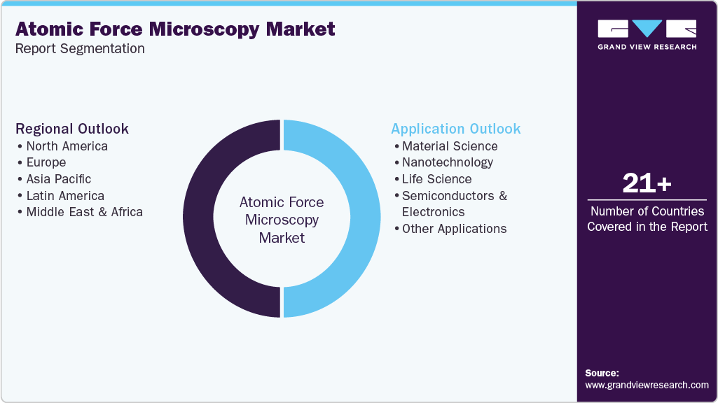
This report forecasts revenue growth at global, regional, and country levels and provides an analysis on industry trends in each of the segments from 2021 to 2033. For this study, Grand View Research, Inc. has segmented the atomic force microscopy market report based on application and region:
-
Application Outlook (Revenue, USD Million, 2021 - 2033)
-
Material Science
-
Nanotechnology
-
Life Science
-
Semiconductors & Electronics
-
Other Applications
-
-
Regional Outlook (Revenue, USD Million, 2021 - 2033)
-
North America
-
U.S.
-
Canada
-
Mexico
-
-
Europe
-
UK
-
Germany
-
France
-
Italy
-
Spain
-
Sweden
-
Denmark
-
Norway
-
-
Asia Pacific
-
China
-
India
-
Japan
-
Australia
-
South Korea
-
New Zealand
-
-
Latin America
-
Brazil
-
Argentina
-
-
MEA
-
South Africa
-
Saudi Arabia
-
Kuwait
-
UAE
-
-
Research Methodology
The atomic force microscopy market figures in this report are based on a proven research process that combines executive interviews with secondary research from proprietary databases, company filings, and recognized regulatory and institutional sources. Market size is built through value-chain sizing-reconciling supply-side and demand-side estimates-and triangulated with bottom-up and top-down approaches. Every estimate passes multiple levels of expert validation before publication, with each atomic force microscopy segment quantified using the revenue-capture definitions in the table below.
Segment Definition
Application
Revenue capture definition
Material Science
Use of AFM to characterize surface morphology, roughness, mechanical properties, adhesion, and nanoscale structure of metals, polymers, ceramics, composites, and advanced materials.
Nanotechnology
Use of AFM for imaging, measuring, manipulating, and analyzing nanoscale structures, nanoparticles, nanomaterials, and nanodevices with high spatial resolution.
Life Science
Use of AFM to study cells, tissues, biomolecules, proteins, DNA, and other biological structures by analyzing their surface morphology, mechanical properties, and molecular interactions.
Semiconductors & Electronics
Use of AFM for nanoscale inspection of wafers, semiconductor surfaces, thin films, integrated circuits, and electronic components, including surface roughness and defect analysis.
Other Applications
Use of AFM across applications such as energy, pharmaceuticals, environmental research, food science, forensic analysis, and industrial quality control where nanoscale surface characterization is required.
Estimation Model
Section
Key Summary
1.1 Research Approach
Hybrid research approach combining secondary and primary research methodologies. Market assessment is based on AFM system revenues, unit shipments, average selling prices (ASP), installation base, replacement demand, application adoption, research and industrial spending, and technology developments. Insights from AFM manufacturers, distributors, semiconductor companies, materials research institutes, universities, nanotechnology laboratories, and industry experts are used to validate market estimates.
1.2 Market Estimation Framework
Market size is estimated using three approaches: (1) AFM unit shipment and ASP model, (2) installed-base and replacement-demand model, and (3) key vendor revenue validation model. These approaches are triangulated to determine the overall market size and forecast projections.
1.2.1 Demand Model
Estimates market demand based on the number of research and industrial laboratories, semiconductor and electronics manufacturing activity, nanotechnology research, materials science applications, life science research, AFM installations, replacement cycles, and adoption of advanced AFM techniques such as high-speed AFM, conductive AFM, scanning tunneling microscopy (STM), AFM-Raman, TERS, and nano-IR.
1.2.2 Revenue Model
Market value is calculated based on AFM system sales, average selling prices, configuration and technology complexity, number of systems sold, software and accessories, service and maintenance revenues, and variations across research, industrial, semiconductor, academic, and other end-use environments.
1.2.3 Vendor Model
Market estimates are validated using revenues of key AFM manufacturers, unit shipments, product portfolios, installed base, new product launches, geographic expansion, acquisitions, partnerships, and financial disclosures of leading companies.
1.3 Forecast Development
Forecast projections are developed by analyzing increasing demand for nanoscale characterization, semiconductor miniaturization, growth of nanotechnology research, advances in materials science, expansion of life science applications, development of 2D materials, adoption of automated and AI-enabled AFM systems, increasing demand for multimodal characterization, and replacement of conventional/older microscopy systems.
1.4 Segmentation Method
Market segmentation is determined using weighted analysis of AFM technology adoption, application requirements, material and sample characteristics, end-user spending, research and industrial activity, semiconductor manufacturing trends, installed equipment base, replacement cycles, system complexity, and regional investment in nanotechnology and advanced materials research.
1.5 Scope & Assumptions
Market measured in USD based on revenues generated from atomic force microscopy systems and associated equipment used for nanoscale surface characterization, imaging, measurement, and analysis. Estimates incorporate AFM system sales, ASPs, unit volumes, installed base, replacement demand, application adoption, technology upgrades, software/accessory revenues where applicable, and regional variations in research and industrial investment.
Delivered Customizations
This report has been delivered with the following In-depth customizations
Client Request
Customization Delivered
Value Adds
AFM Installed Base & Replacement Analysis
Assessment of the installed AFM base, equipment age, replacement cycles, technology upgrades, and demand for next-generation systems across major end users and regions.
Helps clients estimate replacement-driven demand and identify opportunities for upgrades and system modernization.
AFM ASP & Product Tier Analysis
Analysis of AFM systems by entry-level, mid-range, and high-end/premium systems, including typical applications, features, and pricing/ASP ranges.
Helps optimize product positioning, pricing strategy, and portfolio mix.
AFM Technology & Mode Analysis
Assessment of AFM technologies/modes including contact, tapping/non-contact, conductive AFM, high-speed AFM, AFM-Raman, TERS, and nano-IR based on applications, adoption, and technological development.
Helps clients identify high-value technologies and future product opportunities.
Application × Technology Opportunity Matrix
Mapping AFM technologies against applications-for example, AFM-Raman × materials science, high-speed AFM × life sciences, advanced AFM × semiconductors.
Provides a clear view of technology white spaces and emerging application opportunities.
Service & Recurring Revenue Analysis
Assessment of opportunities in AFM installation, calibration, maintenance, repair, software upgrades, accessories, probes, and consumables.
Helps manufacturers identify opportunities to expand recurring and aftermarket revenue.
Frequently Asked Questions About This Report
The global atomic force microscopy market size was estimated at USD 919.2 million in 2025 and is projected to grow from USD 993.0 million in 2026.
The factors driving the market include growing demand for high-resolution surface characterization and nanoscale imaging across materials science, semiconductors, life sciences, nanotechnology, and pharmaceuticals.
Key players in the market include Bruker, KEYENCE CORPORATION, Park Systems, Hitachi High-Tech Corporation, JEOL USA, Inc., Oxford Instruments, HORIBA, Nanosurf, Flash Photonics, Inc., attocube systems GmbH.
Asia Pacific is the fastest-growing region over the forecast period.
The atomic force microscopy market is expected to grow at a CAGR of 8.7% from 2026 to 2033, reaching USD 1,780.9 million by 2033.
The semiconductors & electronics segment accounted for the largest market revenue share of 32.4% in 2025. The rapid miniaturization of semiconductor devices and increasing complexity of advanced chip architectures are driving demand for AFM as manufacturers require highly precise nanoscale characterization and process-control technologies.
North America dominated the market with a revenue share of 38.9% in 2025.
About the Author(s)
Medical Devices Research Team
Healthcare · Medical DevicesThis report was authored by the medical devices research team at Grand View Research - comprising two research analysts, one senior research analyst, and one industry expert - with specialized expertise in the medical devices segment of the healthcare industry. All findings are based on proprietary healthcare databases, executive interviews, and regulatory analysis, subject to internal peer review prior to publication.
Last Updated:
Speak to Analyst


Customize this report to your needs — add regions, segments, or data points, with 20% free customization.
Or view our licence options:


ISO 9001:2015 & 27001:2022 Certified
We are GDPR and CCPA compliant! Your transaction & personal information is safe and secure. For more details, please read our privacy policy.


