
- Home
- »
- Advanced Interior Materials
- »
-
Laser Debonding Equipment Market Size Report, 2026-2033GVR Report cover

Laser Debonding Equipment Market (2026 - 2033)
Size, Share & Trends Analysis Report By Technology (Laser Ablation, Laser-Induced Forward Transfer), By Laser Type (UV Laser, IR Laser), By Application, By Region, And Segment Forecasts
Market Size, 2025
$2.4BMarket Estimate, 2026
$2.5BMarket Forecast, 2033
$3.9BCAGR, 2026–2033
6.5%Laser Debonding Equipment Market Summary
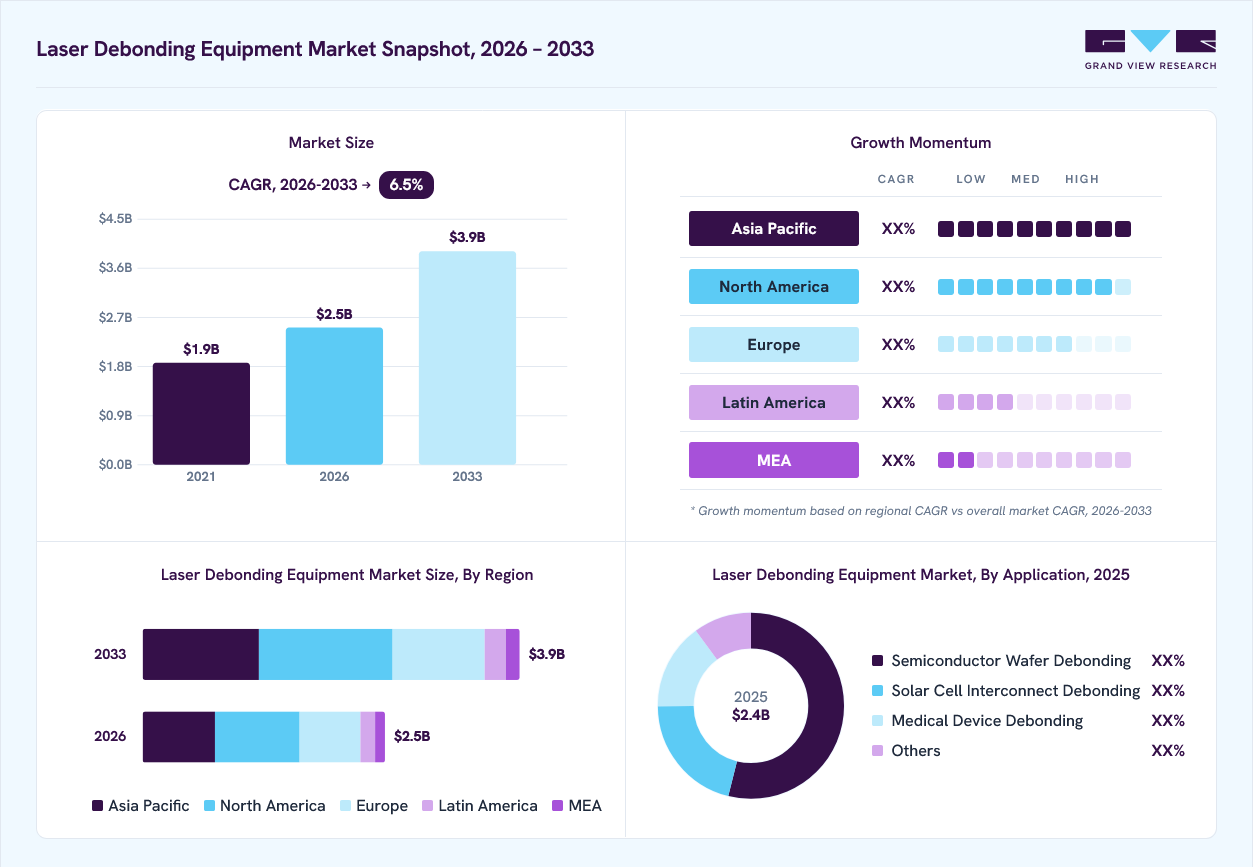
The global laser debonding equipment market size was valued at USD 2.4 billion in 2025 and is projected to grow from USD 2.5 billion in 2026 to USD 3.9 billion by 2033, at a CAGR of 6.5% from 2026 to 2033. The market in North America dominated with a revenue share of 34.9% in 2025. Laser debonding technology is becoming increasingly popular due to its precision, efficiency, and application in industries like semiconductors, solar energy, and medical devices.
 Source: Grand View Research, IR Documents, Primary Interviews, Paid DatabasesTo learn more about this report,
 Download Free Sample Report
Key Market Trends & Insights
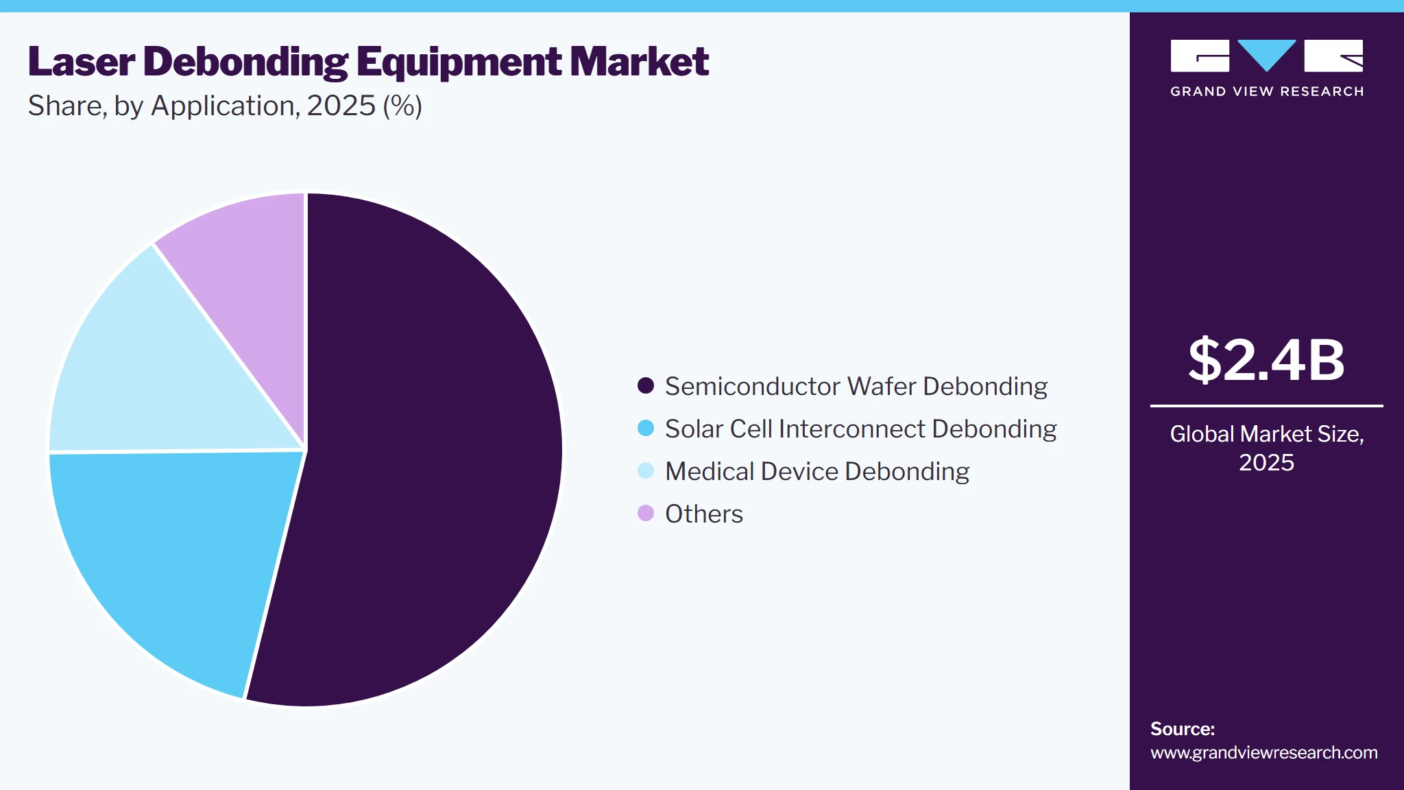
- By application: Semiconductor wafer debonding segment held the largest market share of 53.9% in 2025.
- By technology: Laser ablation segment held the largest market share of 46.0% in 2025.
- By laser type: Ultraviolet (UV) laser segment held the largest market share of 39.0% in 2025.
Regional Highlights
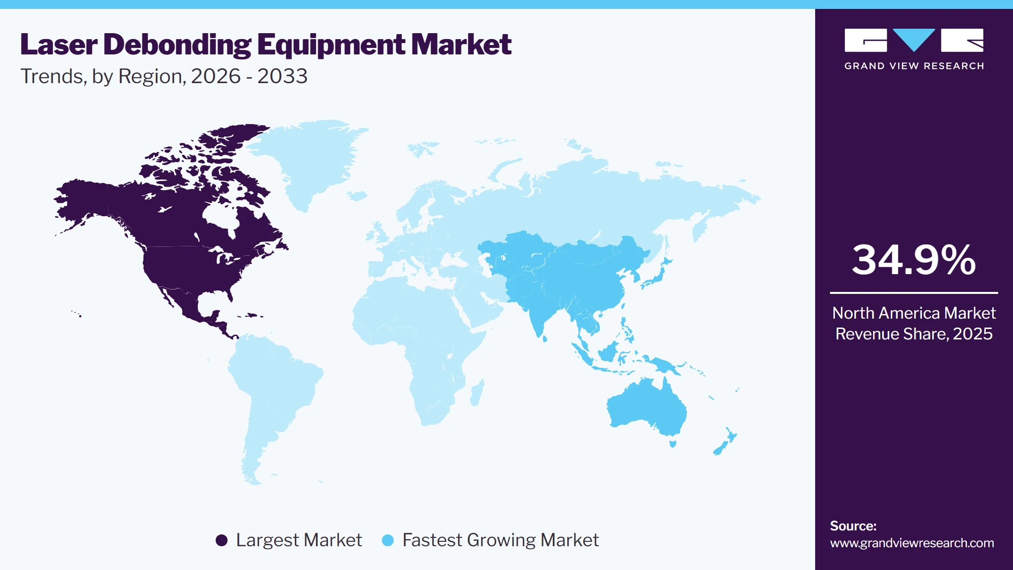
- Largest regional market: North America (34.9% revenue share, 2025)
- Fastest-growing regional market: Asia Pacific (highest CAGR, 2026-2033)
- By country: The U.S. held the largest market share in 2025
Market Size & Forecast
- Market size in 2025: USD 2.4 Billion
- Estimated market size in 2026: USD 2.5 Billion
- Projected market size by 2033: USD 3.9 Billion
- CAGR (2026-2033): 6.5%
GVR research-powered AIAsk Prism AI about the laser debonding equipment marketGet cited answers from GVR research on market growth, segments, regulations and forecasts.Start with✓ Source-linked answers ✓ Market-specific context ✓ Traceable figuresExplore Prism AI ↗
The ability of laser systems to debond materials without causing damage to sensitive components is a key factor driving demand. The laser debonding process is essential in applications where traditional mechanical debonding methods are not effective, offering high precision and low material wastage. It is widely adopted in industries that require intricate material handling, such as semiconductor wafer debonding and medical device debonding. The market is poised to witness strong growth due to increasing advancements in laser technologies and expanding applications in industrial processes.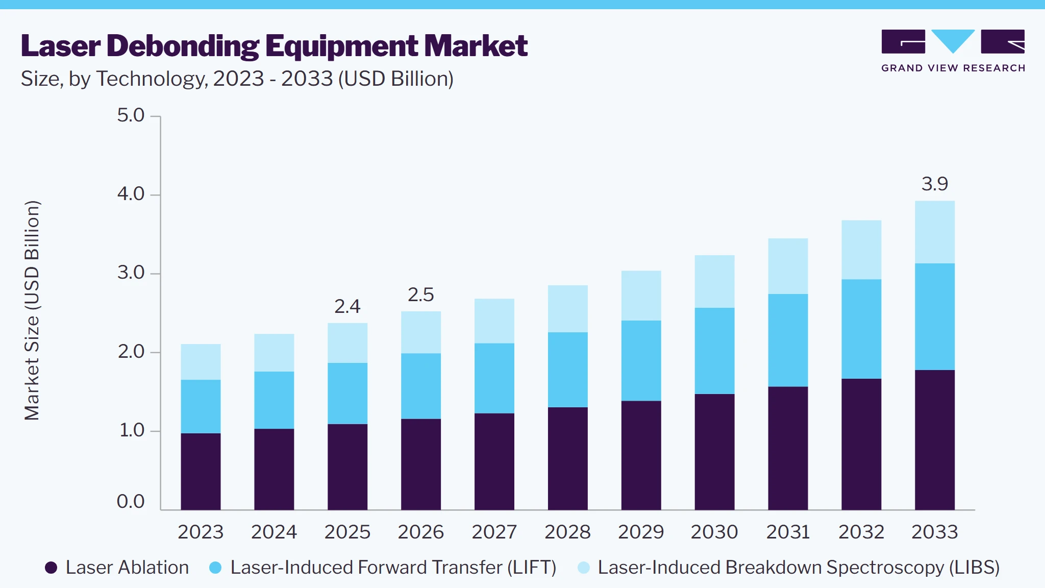 To learn more about this report, Download Free Sample Report
Technological advancements are driving innovation in laser Debonding equipment, with newer technologies such as Laser-Induced Breakdown Spectroscopy (LIBS), laser ablation, and Laser-Induced Forward Transfer (LIFT) becoming more prevalent. These technologies offer greater precision, faster processing times, and improved material handling capabilities. The development of multi-functional laser systems that can handle complex tasks like wafer debonding and solar cell interconnect debonding in a single process step is pushing the boundaries of efficiency and scalability in the market.
The primary drivers of the market include the growing demand for advanced semiconductor manufacturing, increased adoption in renewable energy sectors such as solar, and rising needs for miniaturized, high-performance medical devices. As industries prioritize precision, efficiency, and environmental sustainability, laser debonding technology is becoming increasingly essential in achieving these objectives.
Opportunities for market growth are largely driven by innovations in laser technology, particularly in terms of material processing capabilities. The development of versatile laser Debonding systems capable of handling various applications across semiconductor, medical, and solar industries presents significant market potential. In addition, the rise in automation and AI-enabled systems to enhance operational efficiency is creating further opportunities for market expansion.
Market Dynamics
Advancements in semiconductor packaging, display manufacturing, and microelectronics production is fueling the laser debonding equipment market globally. The increasing adoption of wafer-level packaging, 3D integrated circuits, and advanced chip manufacturing processes is supporting demand for precise and non-contact debonding technologies. Laser debonding equipment offers improved process accuracy, reduced substrate damage, and compatibility with thin wafers and advanced materials. Growing investments in semiconductor fabrication facilities and electronics manufacturing are further contributing to market expansion. However, high equipment costs and technical complexity may limit adoption. Opportunities are emerging from advanced packaging technologies, heterogeneous integration, and expanding semiconductor manufacturing capacity.
The laser debonding equipment market is primarily driven by the increasing adoption of advanced semiconductor packaging technologies. As semiconductor devices become smaller and more complex, manufacturers are adopting wafer-level packaging, 2.5D and 3D integration, and heterogeneous packaging techniques to improve performance and reduce device size. These advanced manufacturing processes often require temporary wafer bonding and precise debonding during production. Laser debonding equipment provides a non-contact process that minimizes mechanical stress and reduces the risk of wafer damage, making it suitable for handling ultra-thin wafers and sensitive substrates. The growing production of high-performance computing chips, artificial intelligence processors, advanced memory devices, and mobile electronics is increasing demand for reliable debonding solutions. Semiconductor manufacturers are also investing in production efficiency and higher yields, encouraging the adoption of laser-based technologies. As advanced packaging continues to gain importance across the electronics industry, demand for laser debonding equipment is expected to strengthen significantly.
Laser debonding equipment incorporates sophisticated laser sources, precision optical components, automation systems, and process control technologies, resulting in significant equipment costs. In addition to the initial investment, manufacturers must ensure compatibility with existing wafer bonding materials, substrate types, and production workflows, which may require additional engineering and process optimization. Operating these systems also requires skilled personnel and regular maintenance to maintain precision and production efficiency. Smaller semiconductor manufacturers and packaging facilities may hesitate to adopt advanced laser debonding technologies due to financial constraints and technical complexity. Long qualification periods and stringent reliability requirements in semiconductor manufacturing can further extend equipment adoption cycles. These factors may affect the pace of market expansion, particularly in cost-sensitive manufacturing environments.
Governments and private companies are investing heavily in new fabrication facilities and advanced packaging plants to strengthen semiconductor supply chains and support increasing demand for electronic devices. Heterogeneous integration, chiplet architectures, and high-density packaging technologies are becoming more common in applications such as artificial intelligence, data centers, automotive electronics, and high-performance computing. These manufacturing approaches require precise temporary bonding and debonding processes to handle increasingly complex wafer structures. Laser debonding technology provides high accuracy, reduced substrate damage, and compatibility with advanced packaging materials, making it suitable for these emerging applications. Technological improvements in laser systems, automation, and process monitoring are further enhancing production efficiency and equipment performance. As semiconductor manufacturers continue to invest in advanced packaging capabilities and next-generation device architectures, the demand for laser debonding equipment is expected to create significant long-term growth opportunities.
Analyst Perspective
The laser debonding equipment market is expected to benefit from the increasing adoption of advanced semiconductor packaging and wafer-thinning technologies. Demand is being driven by the production of high-performance chips for artificial intelligence, high-performance computing, consumer electronics, and automotive applications. Semiconductor wafer debonding is likely to remain the largest application segment, while ultraviolet and pulsed laser systems are gaining traction for their precision and low thermal impact. Market competition is increasingly centered on process accuracy, automation, and compatibility with advanced packaging materials. Companies with strong semiconductor ecosystem partnerships and laser engineering expertise are expected to strengthen their market positions.
Technology Insights
Based on technology, the laser ablation segment led the market with the largest revenue share of 46.0% in 2025. Laser Ablation, which involves removing material using laser beams, is widely used in medical device debonding and semiconductor processes. Its precision and non-contact nature make it ideal for applications that demand minimal material damage during debonding. As industries move towards more precise manufacturing processes, the demand for laser ablation technology is expected to grow rapidly.
The laser-induced forward transfer (LIFT) segment is expected to grow at a CAGR of 7.2% over the forecast period, owing to its high-precision material deposition, ideal for complex 3D microstructures in electronics and biomedicine. In addition, its ability to handle solid/liquid phases without clogging meets the demand for miniaturization and customization.
Laser Type Insights
Based on laser type, the ultraviolet (UV) laser segment led the market with the largest revenue share of 39.0% in 2025. Ultraviolet (UV) lasers are known for their short wavelength, enabling precise material removal with minimal thermal impact. UV lasers are widely used in applications requiring fine feature debonding, such as semiconductor wafer debonding and medical device fabrication. The ability of UV lasers to process materials with high accuracy and reduced damage to surrounding components makes them highly suitable for industries where precision and quality are paramount.
Pulsed lasers are expected to grow at a CAGR of 6.8% over the forecast period. Pulsed lasers offer high peak power in short bursts, making them ideal for precision debonding applications in industries such as semiconductors and medical devices. Pulsed lasers are effective in applications that require controlled energy delivery, allowing for precise material removal without damaging surrounding areas. The growing trend of miniaturization and the increasing demand for precision-driven applications are boosting the adoption of pulsed laser technology in the market.
Application Insights
Based on application, the semiconductor wafer debonding segment led the market with the largest revenue share of 53.9% in 2025, driven by the rapid advancements in semiconductor technology. As the demand for smaller and more efficient electronic devices grows, the need for precise debonding of wafer layers is becoming critical. Laser debonding equipment offers high precision and speed in semiconductor wafer debonding, reducing the risk of damage to delicate components and improving production efficiency.
 To learn more about this report, Download Free Sample Report
The medical device debonding is expected to grow at a significant CAGR of 6.7% from 2026 to 2033, owing to the growing demand for advanced medical devices and equipment, owing to the growing demand for advanced medical devices and equipment. Laser debonding technology enables precise and controlled removal of materials in medical devices, ensuring high-quality end products. The increasing trend toward miniaturized medical devices and the need for precision in manufacturing processes are contributing to the growth of this application.
Regional Insights
North America dominated the laser debonding equipment market with the largest revenue share of 34.9% in 2025, with the U.S. leading in terms of adoption and innovation. The region's robust semiconductor industry, combined with advancements in medical device manufacturing, is driving demand for laser debonding equipment. The presence of key market players and high R&D investments in new laser technologies further contribute to the market's growth in North America.
 To learn more about this report, Download Free Sample Report
U.S. Laser Debonding Equipment Market Trends
The laser debonding equipment market in the U.S. held the largest share in the North America region in 2025, driven by its advanced technological infrastructure and a strong presence in semiconductor and medical device manufacturing. The country's focus on innovation, coupled with significant R&D investments, is driving the development and adoption of cutting-edge laser Debonding technologies. The U.S. also benefits from a well-established industrial base, contributing to the continued market growth.
Asia Pacific Laser Debonding Equipment Market Trends
Asia Pacific laser debonding equipment market is expected to grow at the fastest CAGR of 7.0% over the forecast period, owing to rapid industrialization and the increasing demand for advanced semiconductor manufacturing technologies. Countries like China, Japan, and South Korea are major hubs for electronics production, driving demand for high-precision laser debonding systems. The growing emphasis on renewable energy in the region is also contributing to the market's expansion, particularly in solar cell manufacturing.
The laser debonding equipment market in China led the Asia Pacific market with the largest revenue share in 2025, due to its vast electronics manufacturing base. The push for smaller devices and advanced semiconductor packaging boosts the need for precise debonding.
Europe Laser Debonding Equipment Market Trends
The European laser debonding equipment market is expected to remain strong, particularly in industries such as pharmaceuticals, automotive, and renewable energy. The region's focus on environmental sustainability and its well-established manufacturing base in high-tech industries contribute to the increasing adoption of laser Debonding systems. Countries such as Germany, France, and the UK are key players in the European market due to their emphasis on innovation and precision-driven manufacturing.
The laser debonding equipment market in Germany is expected to grow significantly, driven by its prominent automotive and electronics sectors. In addition, the surge in electric vehicles and autonomous systems increases the demand for laser debonding in battery and electronics production.
Key Laser Debonding Equipment Company Insights
Some of the key players operating in the global market include Shin-Etsu Engineering Co., LTD., EV Group (EVG), SUSS MicroTec SE, CWI Technical, Kingyoup Enterprises Co., Ltd, Optec S.A., among others.
-
SUSS MicroTec SE specializes in photolithography, wafer bonding, and laser Debonding technologies. The company’s laser Debonding systems are used in applications such as wafer-level packaging and advanced semiconductor processing, where precision and throughput are critical
-
EV Group (EVG) is a global leader in wafer bonding, lithography, and metrology equipment for the semiconductor, MEMS, and nanotechnology markets. The company’s portfolio includes advanced laser Debonding systems designed for high-precision applications in semiconductor wafer processing and MEMS manufacturing. EVG is renowned for its innovation and customization capabilities, offering flexible solutions that cater to both large-scale production and specialized, niche markets
-
Shin-Etsu Engineering Co., LTD. specializes in advanced material processing technologies that cater to industries such as semiconductors, electronics, and solar energy. Shin-Etsu's laser debonding equipment is recognized for its precision, reliability, and ability to handle complex wafer debonding processes.
Key Laser Debonding Equipment Companies:
The following key companies have been profiled for this study on the laser debonding equipment market.
-
Shin-Etsu Engineering Co., LTD.
-
EV Group (EVG)
-
SUSS MicroTec SE
-
CWI Technical
-
Kingyoup Enterprises Co., Ltd
-
Optec S.A.
-
Brewer Science, Inc.
-
Tokyo Electron Limited
-
SuperbIN Co. Ltd.
-
Han's Laser Technology Industry Group Co., Ltd
Competitive Benchmarking
Category
Operating Strategies
Competitive Edge
Weakness
Established Players (e.g. Tokyo Electron Limited, EV Group (EVG), SUSS MicroTec SE, Shin-Etsu Engineering Co., Ltd., Brewer Science, Inc.
- Focus on expanding laser debonding equipment portfolios for advanced semiconductor packaging, wafer-level processing, and microelectronics manufacturing.
- Invest in high-precision laser technologies, automation, and integrated process control systems.
- Strengthen collaborations with semiconductor foundries, OSAT companies, and electronics manufacturers.
- Strong technological expertise in precision laser processing and semiconductor manufacturing equipment.
- Broad product portfolios with advanced engineering and process integration capabilities.
- Established relationships with global semiconductor and electronics manufacturers.
- High research, development, and equipment manufacturing costs.
- Dependence on semiconductor capital expenditure and technology investment cycles.
- Long product qualification and adoption timelines in advanced manufacturing environments.
Emerging & Regional Players (e.g Han's Laser Technology Industry Group Co., Ltd., SuperbIN Co., Ltd., Kingyoup Enterprises Co., Ltd., CWI Technical, Optec S.A.)
- Focus on specialized and application-specific laser debonding solutions for niche semiconductor and electronics applications.
- Expand presence through customized equipment development and regional partnerships.
- Emphasize flexible system designs for evolving advanced packaging requirements.
- Competitive pricing and greater flexibility in customized equipment development.
- Ability to address specialized manufacturing requirements and emerging applications.
- Agile operations enabling quicker response to changing customer needs.
- Limited financial capacity for large-scale research and advanced laser technology development.
- Smaller global sales and service networks compared with established competitors.
- Lower participation in high-volume semiconductor manufacturing projects and advanced packaging ecosystems.
Recent Developments
-
In June 2024, EV Group (EVG), a prominent provider of wafer bonding and lithography equipment for the MEMS, nanotechnology, and semiconductor industries, announced a strategic partnership with Fraunhofer IZM-ASSID (All Silicon System Integration Dresden), a division of Fraunhofer IZM known for its cutting-edge research in 3D wafer-level system integration. Together, they aim to develop and optimize alternative bonding and debonding technologies for advanced CMOS and heterogeneous integration applications, including quantum computing.
-
In May 2024, EV Group announced a significant advancement in its semiconductor layer transfer technology, doubling its throughput. EVG's LayerRelease technology employs an IR laser and inorganic release materials to achieve laser debonding on silicon carriers with nanometer-level precision in production environments. This approach effectively resolves issues related to temperature sensitivity and glass carrier compatibility. By eliminating the need for glass substrates and organic adhesives, the innovative process ensures compatibility with front-end processes for ultra-thin layer transfer and subsequent downstream operations.
Laser Debonding Equipment Market Report Scope
Report Attribute
Details
Market size in 2025
USD 2.4 billion
Estimated market size in 2026
USD 2.5 billion
Projected market size by 2033
USD 3.9 billion
Growth rate
CAGR of 6.5% from 2026 to 2033
Base year for estimation
2025
Historical data
2021 - 2024
Forecast period
2026 - 2033
Quantitative units
Revenue in USD billion and CAGR from 2026 to 2033
Report coverage
Revenue forecast, company ranking, competitive landscape, growth factors, and trends
Segments covered
Technology, laser type, application, region
Regional scope
North America; Europe; Asia Pacific; Latin America; Middle East & Africa
Country scope
U.S.; Canada; Mexico; U.K.; Germany; France; Italy; Spain; China; India; Japan; Australia; South Korea; Brazil; Argentina; Saudi Arabia, UAE; South Africa
Key companies profiled
Shin-Etsu Engineering Co., LTD.; EV Group (EVG); SUSS MicroTec SE; CWI Technical; Kingyoup Enterprises Co., Ltd; Optec S.A.; Brewer Science, Inc.; Tokyo Electron Limited; SuperbIN Co. Ltd.; Han's Laser Technology Industry Group Co., Ltd
Customization scope
Free report customization (equivalent up to 8 analysts' working days) with purchase. Addition or alteration to country, regional & segment scope.
Pricing and purchase options
Avail customized purchase options to meet your exact research needs. Explore purchase options
Global Laser Debonding Equipment Market Report Segmentation
This report forecasts revenue growth at global, regional, and country levels and analyzes the latest industry trends in each sub-segment from 2021 to 2033. For this study, Grand View Research has segmented the global laser debonding equipment market report based on, technology, laser type, application, and region.
 To learn more about this report, Download Free Sample Report
-
Technology Outlook (Revenue, USD Million, 2021 - 2033)
-
Laser-Induced Breakdown Spectroscopy (LIBS)
-
Laser Ablation
-
Laser-Induced Forward Transfer (LIFT)
-
-
Laser Type Outlook (Revenue, USD Million, 2021 - 2033)
-
Ultraviolet (UV) Laser
-
Infrared (IR) Laser
-
Pulsed Laser
-
Others
-
-
Application Outlook (Revenue, USD Million, 2021 - 2033)
-
Semiconductor Wafer Debonding
-
Solar Cell Interconnect Debonding
-
Medical Device Debonding
-
Others
-
-
Regional Outlook (Revenue, USD Million, 2021 - 2033)
-
North America
-
U.S.
-
Canada
-
Mexico
-
-
Europe
-
Germany
-
France
-
Italy
-
Spain
-
UK
-
-
Asia Pacific
-
China
-
India
-
Japan
-
South Korea
-
Australia
-
-
Latin America
-
Brazil
-
Argentina
-
-
Middle East and Africa
-
Saudi Arabia
-
UAE
-
South Africa
-
-
Research Methodology
The laser debonding equipment market figures in this report are based on a proven research process that combines executive interviews with secondary research from proprietary databases, company filings, and recognized regulatory and institutional sources. Market size is built through value-chain sizing - reconciling supply-side and demand-side estimates - and triangulated with bottom-up and top-down approaches. Every estimate passes multiple levels of expert validation before publication, with each laser debonding equipment segment quantified using the revenue-capture definitions in the table below.
Segment Definition
Segment - Technology
Revenue Capture Definition
Laser-Induced Breakdown Spectroscopy (LIBS)
Revenue is generated from laser debonding equipment employing LIBS technology for precise material separation and process monitoring in semiconductor, electronics, and advanced manufacturing applications.
Laser Ablation
Revenue is captured through laser ablation systems that remove bonding layers using controlled laser energy for wafer processing and microelectronics manufacturing, supporting high-precision debonding operations.
Laser-Induced Forward Transfer (LIFT)
Revenue is generated from LIFT-based laser debonding equipment used for transferring and separating thin materials in semiconductor packaging, microfabrication, and advanced electronics production processes.
Segment - Laser Type
Revenue Capture Definition
Ultraviolet (UV) Laser
Revenue is generated through UV laser debonding systems used for high-precision material processing and temporary wafer debonding applications requiring minimal thermal impact and substrate damage.
Infrared (IR) Laser
Revenue is captured through IR laser debonding equipment designed for efficient removal of bonding layers in semiconductor and electronics manufacturing requiring deeper material penetration.
Pulsed Laser
Revenue is generated from pulsed laser systems that provide controlled energy delivery for accurate debonding processes across semiconductor packaging, electronics, and precision manufacturing applications.
Others
Revenue is captured through other laser technologies used for specialized debonding applications across advanced manufacturing, research, and industrial processing requiring customized laser solutions.
Segment -
Application
Revenue Capture Definition
Semiconductor Wafer Debonding
Revenue is generated through laser debonding equipment used for temporary wafer separation in advanced semiconductor packaging, wafer-level processing, and three-dimensional integrated circuit manufacturing.
Solar Cell Interconnect Debonding
Revenue is captured through laser debonding systems used in solar cell manufacturing for separating bonded layers and improving production precision during photovoltaic module fabrication.
Medical Device Debonding
Revenue is generated from laser debonding equipment used in the manufacturing of medical devices requiring precise material separation and high-quality microfabrication processes.
Others
Revenue is captured through laser debonding equipment used across electronics, displays, research, aerospace, and other advanced manufacturing applications requiring precise and non-contact debonding technologies.
Estimation Model
Layer Name
Key Question
Description
Advanced Electronics Manufacturing Layer
Which industries generate demand for laser debonding equipment?
The estimation begins by evaluating production activities across semiconductor manufacturing, solar cell production, medical device fabrication, and other precision electronics industries. Growth in advanced packaging and microfabrication establishes the base market demand.
Laser Debonding Technology Adoption Layer
Which debonding technologies drive market demand?
This layer refines demand by assessing the adoption of Laser-Induced Breakdown Spectroscopy (LIBS), Laser Ablation, and Laser-Induced Forward Transfer (LIFT) technologies. Process precision, substrate compatibility, and manufacturing requirements influence technology selection.
Laser Type and Application Deployment Layer
What determines equipment installations?
Market demand is estimated through the adoption of ultraviolet (UV), infrared (IR), pulsed, and other laser systems across semiconductor wafer debonding, solar cell interconnect debonding, medical device manufacturing, and other advanced applications. Capacity expansions and equipment replacement further support demand.
Revenue Layer
How is total market revenue calculated?
Revenue is estimated by aggregating laser debonding equipment sales across technologies, laser types, applications, and regional markets. Semiconductor fabrication investments, advanced packaging capacity additions, equipment pricing, replacement cycles, and manufacturer revenues are incorporated to validate the total market size.
Delivered Customizations
This report has been delivered with the following In-depth customizations
CLIENT REQUEST
CUSTOMIZATION DELIVERED
VALUE ADDS
Regional Segmentation
Detailed regional analysis covered North America, Europe, Asia Pacific, Latin America, and the Middle East & Africa, with country-level assessment of key markets. The study evaluated semiconductor fabrication capacity, advanced packaging activities, electronics manufacturing, solar cell production, medical device manufacturing, and government investments influencing laser debonding equipment demand.
Helped identify high-growth regions, country-specific opportunities, and evolving demand trends across semiconductor, electronics, solar, and medical device industries, supporting market entry strategies, regional expansion planning, and identification of emerging advanced manufacturing hubs.
Competitive Benchmarking
Comprehensive benchmarking assessed major participants based on product portfolio, laser debonding technologies, engineering capabilities, manufacturing strength, automation features, regional presence, pricing strategies, aftermarket services, and distribution networks. The study also compared established and emerging players in the laser debonding equipment market.
Assisted clients in evaluating competitor positioning, technology capabilities, and market gaps while supporting strategic planning, partnership opportunities, product differentiation, and investment decisions across semiconductor packaging and precision manufacturing applications.
Opportunity Assessment
In-depth opportunity assessment analyzed semiconductor fabrication expansions, advanced packaging investments, heterogeneous integration, wafer-level manufacturing, and growth in electronics and photovoltaic industries. The study identified emerging opportunities in high-precision laser processing, automated debonding systems, and next-generation semiconductor manufacturing technologies.
Enabled clients to identify high-growth investment areas, prioritize regional expansion, and evaluate future revenue opportunities while supporting product development, technology adoption, and long-term growth strategies in the laser debonding equipment market.
Frequently Asked Questions About This Report
The ultraviolet (UV) laser segment led the market with the largest revenue share of 39.0% in 2025.
The laser ablation segment dominated the market and accounted for the largest revenue share of 46.0% in 2025.
Major end users include the semiconductor industry, electronics manufacturing companies, advanced packaging facilities, MEMS manufacturers, and research institutions involved in microelectronics fabrication.
Key trends include the increasing adoption of UV lasers for precision processing, growing demand for temporary bonding and debonding technologies in advanced packaging, expansion of AI and high-performance computing chips, and rising investments in next-generation semiconductor fabrication facilities.
The global laser debonding equipment market size was valued at USD 2.4 billion in 2025 and is expected to reach USD 2.5 billion in 2026.
The global laser debonding equipment market, in terms of revenue, is expected to grow at a compound annual growth rate of 6.5% from 2026 to 2033, reaching USD 3.9 billion by 2033.
North America dominated the laser debonding equipment market with a revenue share of 34.9% in 2025. The region's robust semiconductor industry, combined with advancements in medical device manufacturing, is driving demand for laser debonding equipment.
Some of the key players operating in the laser debonding equipment market include Shin-Etsu Engineering Co., LTD., EV Group (EVG), SUSS MicroTec SE, CWI Technical, Kingyoup Enterprises Co., Ltd, Optec S.A., Brewer Science, Inc., Tokyo Electron Limited, SuperbIN Co. Ltd., Han's Laser Technology Industry Group Co., Ltd.
The laser debonding equipment market is fueled by growing demand for advanced semiconductor manufacturing, increased adoption in renewable energy sectors such as solar, and rising needs for miniaturized, high-performance medical devices.
About the Author(s)
Advanced Interior Materials Research Team
Advanced Materials · Advanced Interior MaterialsThis report was authored by the advanced interior materials research team at Grand View Research - comprising two research analysts, one senior research analyst, and one industry expert - with specialized expertise in the advanced interior materials segment of the advanced materials industry. All findings are based on proprietary advanced materials databases, executive interviews, and regulatory analysis, subject to internal peer review prior to publication.
Last Updated:
Speak to Analyst

Customize this report to your needs - add regions, segments, or data points, with 20% free customization.
Or view our licence options:


ISO 9001:2015 & 27001:2022 Certified
We are GDPR and CCPA compliant! Your transaction & personal information is safe and secure. For more details, please read our privacy policy.


