- Home
- »
- Advanced Interior Materials
- »
-
Semiconductor Defect Inspection Equipment Market Report, 2033GVR Report cover
![Semiconductor Defect Inspection Equipment Market Size, Share & Trends Report]()
Semiconductor Defect Inspection Equipment Market (2025 - 2033) Size, Share & Trends Analysis Report By Defect (Metal Defect Inspection), By Technology (Optical Inspection), By Process Stage, By Inspection Technique, By End Use, By Region, And Segment Forecasts
- Report ID: GVR-4-68040-681-9
- Number of Report Pages: 100
- Format: PDF
- Historical Range: 2021 - 2023
- Forecast Period: 2025 - 2033
- Industry: Advanced Materials
- Report Summary
- Table of Contents
- Interactive Charts
- Methodology
- Download FREE Sample
-
Download Sample Report
Semiconductor Defect Inspection Equipment Market Summary
The global semiconductor defect inspection equipment market size was estimated at USD 5,603.5 million in 2024 and is projected to reach USD 12,154.3 million by 2033, growing at a CAGR of 9.0% from 2025 to 2033. The increasing complexity of semiconductor devices, driven by the miniaturization of chips and the adoption of advanced nodes (e.g., 5nm and below), has significantly raised the demand for high-precision defect inspection equipment.
Key Market Trends & Insights
- Asia Pacific dominated the semiconductor defect inspection equipment market with the largest revenue share of 67.0% in 2024.
- The semiconductor defect inspection equipment market in the U.S. is expected to grow at a substantial CAGR of 7.2% from 2025 to 2033.
- By defect, the metal defect inspection segment is expected to grow at a considerable CAGR of 9.7% from 2025 to 2033 in terms of revenue.
- By technology, the optical inspection segment is expected to grow at a considerable CAGR of 9.5% from 2025 to 2033 in terms of revenue.
- By end use, the foundry segment is expected to grow at a considerable CAGR of 9.8% from 2025 to 2033 in terms of revenue.
Market Size & Forecast
- 2024 Market Size: USD 5,603.5 Million
- 2033 Projected Market Size: USD 12,154.3 Million
- CAGR (2025-2033): 9.0%
- Asia Pacific: Largest market in 2024
As device geometries shrink, even the smallest defect can impact functionality, prompting chipmakers to invest heavily in advanced inspection technologies. Moreover, the surge in demand for consumer electronics, AI hardware, 5G infrastructure, and electric vehicles has accelerated semiconductor production volumes, boosting the need for yield management solutions.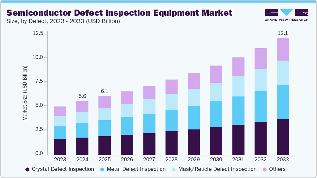
Automated and AI-driven inspection tools are gaining prominence for enabling faster, more accurate defect classification across FEOL and BEOL stages. In addition, governments and private sectors globally are investing in semiconductor fabs, fueling equipment procurement. These factors collectively support the rapid growth of the market across all regions.
Market Concentration & Characteristics
The global semiconductor defect inspection equipment industry is moderately concentrated, with a few major players dominating the landscape. Leading companies hold significant market share due to their advanced technology portfolios and strong customer relationships. High capital requirements and technological barriers limit the entry of new competitors. However, innovation and partnerships continue to shape competition within the industry.
The semiconductor defect inspection equipment industry is highly innovation-driven, fueled by the need for precision at nanoscale levels. Continuous R&D is essential to keep pace with evolving chip architectures and shrinking nodes. Companies invest heavily in advanced techniques such as AI-based analytics and 3D inspection tools. Innovation is a key differentiator and directly influences market leadership.
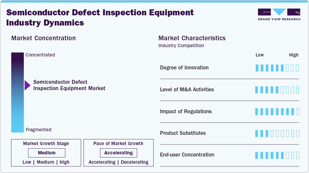
Mergers and acquisitions play a strategic role in the market, enabling firms to expand technological capabilities and customer reach. Larger players often acquire niche technology firms to enhance their inspection solutions and speed up time to market. This trend strengthens competitive positioning and accelerates product development cycles. M&A activities are also used to gain access to specialized talent and patents.
Regulatory compliance impacts the industry, especially regarding equipment safety, export controls, and environmental standards. International trade policies and semiconductor export restrictions can influence equipment supply chains. Vendors must align with regional regulations when deploying tools globally. As geopolitical tensions rise, regulatory scrutiny is expected to increase further.
Drivers, Opportunities & Restraints
The rise in demand for advanced electronics, AI chips, and 5G devices is fueling growth in the semiconductor defect inspection equipment industry. Shrinking transistor sizes and complex architectures require high-precision inspection tools. Increasing investments in semiconductor fabrication facilities globally also support market expansion. In addition, the focus on improving yield and reducing production costs is driving adoption.
Emerging technologies such as quantum computing, autonomous vehicles, and IoT present new growth avenues for inspection equipment vendors. Expansion of semiconductor manufacturing in regions like Southeast Asia and the Middle East offers untapped potential. Adoption of AI and machine learning in inspection processes enhances accuracy and speed. These developments open opportunities for innovation and market penetration.
High equipment costs and complex installation processes pose challenges for small and mid-sized fabs. The industry also faces supply chain disruptions and component shortages, impacting equipment availability. Rapid technology changes demand continuous upgrades, increasing operational costs for end users. In addition, stringent export controls and geopolitical tensions can restrict market access.
Defect Insights
The crystal defect inspection segment dominated the market with a share of 32.1% in 2024, due to its critical role in early-stage wafer quality control. Identifying lattice imperfections and dislocations is essential for ensuring high yield and device reliability. With the continued scaling of nodes, even minor crystal defects can compromise chip performance. As a result, manufacturers prioritize advanced crystal inspection tools in front-end processes.
Metal defect inspection is projected to be the fastest-growing segment over the forecast period, driven by the increasing complexity of metal layers in advanced semiconductor designs. As multi-layer interconnects become denser, detecting voids, residues, and particle contamination becomes more challenging and vital. The adoption of AI and high-resolution imaging technologies is enhancing metal defect detection accuracy. Growing demand for high-performance chips in AI, HPC, and 5G devices is accelerating investment in this area.
Technology Insights
The optical inspection segment accounted for a share of 34.9% in 2024 owing to its speed, cost-efficiency, and wide applicability across process stages. It is widely used for detecting surface-level defects and pattern variations in both FEOL and BEOL. Advancements in resolution and automated analysis have further improved its effectiveness in high-volume manufacturing. Its ability to rapidly scan large wafer areas makes it a preferred choice for production lines.
Electron beam (e-beam) inspection is anticipated to experience significant growth over the forecast period, driven by its ability to detect ultra-small defects that optical systems may miss. It is especially valuable for advanced nodes below 5nm, where defect sizes are increasingly minute. E-beam systems offer high resolution and precision, making them suitable for critical patterning and logic device inspection. Despite slower throughput, its importance is rising in R&D and yield learning applications.
Process Stage Insights
Front-End of Line (FEOL) dominated the market with a 42.6% revenue share in 2024, as it involves the formation of essential device structures on the silicon wafer. Detecting defects early in this phase is critical to preventing costly downstream failures and yield losses. High-precision inspection tools are used extensively to monitor doping, gate formation, and other critical processes. The increasing complexity of transistor architectures has further intensified demand for FEOL inspection solutions.
Packaging and assembly is anticipated to be the fastest-growing segment over the forecast period, due to the rising demand for advanced packaging technologies such as 2.5D, 3D stacking, and chiplet integration. As the industry shifts toward heterogeneous integration, detecting defects in interconnects, micro-bumps, and substrates becomes more critical. Inspection tools that support 3D imaging and internal layer analysis are gaining traction. This trend is driven by the need for high-performance, compact, and thermally efficient semiconductor devices.
Inspection Technique Insights
The 3D inspection techniques segment accounted for a share of 44.2% in 2024owing to their ability to accurately analyze complex, multi-layered semiconductor structures. These techniques are essential for advanced packaging, 3D NAND, and FinFET architectures where traditional 2D methods fall short. They provide critical depth information to detect defects within buried layers and stacked components. As devices become more compact and layered, 3D inspection ensures precise defect localization and quality assurance.
Machine learning and AI-based inspection is projected to be the fastest-growing segment over the forecast period, driven by the need for faster, more adaptive defect detection. These systems learn from large datasets to improve defect classification and reduce false positives. They enable predictive analytics and real-time process control, enhancing yield and operational efficiency. With increasing data complexity in semiconductor manufacturing, AI-powered tools are becoming essential for next-generation inspection.
End Use Insights
The foundry segment held a share of 30.6% in 2024 due to its high-volume manufacturing and advanced process node capabilities. They serve a diverse range of clients, requiring cutting-edge inspection tools to ensure quality and yield across varied designs. Continuous investments in advanced nodes like 5nm and below have boosted demand for precise defect detection technologies. Foundries prioritize inspection at every process stage to meet strict client and performance requirements.
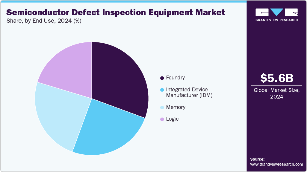
IDMs are witnessing significant growth in defect inspection adoption as they manage both design and manufacturing in-house. With increasing focus on developing proprietary technologies for AI, automotive, and industrial applications, IDMs invest heavily in in-line inspection solutions. Their vertically integrated operations require robust tools across FEOL, BEOL, and packaging. As competition intensifies, IDMs are expanding capacity and upgrading inspection systems to maintain quality and innovation leadership.
Regional Insights
North America semiconductor defect inspection equipment industry is anticipated to grow at a significant CAGR of 7.3% over the forecast period. This growth is due to strong presence of major IDMs and foundries. The U.S. leads in R&D investments and adoption of cutting-edge inspection technologies. Government support for semiconductor manufacturing further boosts regional growth. Ongoing fab expansions and focus on domestic chip production strengthen market dominance.
U.S. Semiconductor Defect Inspection Equipment Market Trends
The U.S. semiconductor defect inspection equipment industry dominated the North American region in the 2024 due to its strong base of IDMs, foundries, and leading equipment manufacturers. Major investments under the CHIPS Act are accelerating domestic semiconductor production. The country is a hub for innovation in AI-driven and high-resolution inspection technologies. Continuous R&D and government support strengthen its leadership position.
Canada semiconductor defect inspection equipment industry is witnessing steady growth, supported by expanding microelectronics and photonics sectors. Research institutions and startups are increasingly exploring AI and advanced manufacturing applications. Government initiatives to boost local tech innovation are enhancing market prospects. Though smaller in scale, Canada’s role in the North American supply chain is growing.
Europe Semiconductor Defect Inspection Equipment Market Trends
Europe semiconductor defect inspection equipment industry is witnessing steady growth driven by investments in semiconductor research and advanced manufacturing. Countries like Germany and the Netherlands are prominent due to the presence of leading equipment manufacturers. EU initiatives to boost semiconductor self-reliance are fostering demand for inspection tools. The region emphasizes high standards in precision and innovation.
Germany semiconductor defect inspection equipment industry plays a key role in the European region due to its strong engineering and manufacturing capabilities. The country is home to leading equipment suppliers and supports advanced semiconductor research. Growth is fueled by rising demand for precision tools in automotive and industrial electronics. Government initiatives to strengthen domestic chip production further support market expansion.
The UK semiconductor defect inspection equipment industry is experiencing growthdriven by investments in R&D and advanced technologies. Emerging startups and collaborations with global semiconductor firms are boosting innovation. Government funding for chip design and inspection capabilities is enhancing local infrastructure. The country's focus on building a resilient semiconductor supply chain contributes to steady market progress.
Asia Pacific Semiconductor Defect Inspection Equipment Market Trends
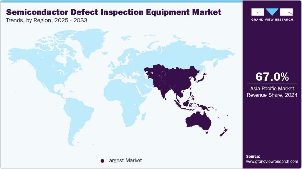
Asia Pacific semiconductor defect inspection equipment industry dominated globally in 2024 and accounted for a 67.0% global share. Countries such as Taiwan, South Korea, China, and Japan dominate global chip production and continue to expand capacity. Strong government backing and high concentration of foundries fuel demand for advanced inspection systems. The region benefits from a robust supply chain and skilled workforce.
Taiwan semiconductor defect inspection equipment industry dominated the Asia Pacific region in 2024 with a35.3% share, driven by its position as a global leader in chip manufacturing. Home to major foundries like TSMC, the country invests heavily in advanced inspection tools to support leading-edge nodes. High production volumes and focus on yield optimization fuel constant demand for precise inspection systems. Taiwan's mature semiconductor ecosystem and skilled workforce further reinforce its market leadership.
China semiconductor defect inspection equipment industry is witnessing rapid growth due to its aggressive push for semiconductor self-sufficiency. Massive investments in domestic fabs and inspection tool capabilities are driving demand. The government’s support through subsidies and policies is fostering local equipment development. Ongoing U.S. export restrictions are further encouraging China to enhance its in-house inspection technology.
Middle East & Africa Semiconductor Defect Inspection Equipment Market Trends
The Middle East and Africa semiconductor defect inspection equipment industryis an emergingmarket with growing interest in semiconductor manufacturing and R&D. Government-led initiatives aim to diversify economies through high-tech industries. While the market is still in early stages, demand for inspection tools is slowly increasing. Collaboration with global players is expected to support future growth.
Israel semiconductor defect inspection equipment industry is experiencing growth, supported by its strong R&D ecosystem and advanced microelectronics sector. The country is home to several global semiconductor firms and innovative startups specializing in inspection and metrology technologies. Government-backed initiatives and international collaborations are boosting infrastructure and capabilities. As demand for AI, defense, and communications chips increases, investment in defect inspection tools continues to rise.
Latin America Semiconductor Defect Inspection Equipment Market Trends
Latin America semiconductor defect inspection equipment industry is experiencing gradual growth in semiconductor-related activities, primarily in testing and assembly operations. Countries like Brazil and Mexico are exploring opportunities to expand electronics manufacturing. While the region lacks major fabs, rising tech adoption drives equipment demand. Growth is expected to accelerate with foreign investment and infrastructure development.
Brazil semiconductor defect inspection equipment industry is experiencing growth due to its expanding electronics and automotive sectors. Government initiatives to promote local semiconductor production are driving demand for advanced inspection tools. Research institutions and industrial hubs are increasingly focusing on microelectronics and chip testing. As domestic manufacturing capabilities improve, the need for precision inspection equipment continues to grow.
Key Semiconductor Defect Inspection Equipment Company Insights
Some of the key players operating in the market include Merck KGaA; KLA Corporation; and Toray Group
-
Honeywell is a diversified global technology and manufacturing company known for its strong presence in building technologies, including HVAC systems and industrial filtration solutions. The company offers a wide range of advanced air filtration products designed to improve indoor air quality and enhance energy efficiency across commercial, industrial, and residential applications. Honeywell’s filtration solutions are integrated with smart building management systems, allowing for real-time monitoring and optimized performance.
-
KLA Corporation is a global leader in diversified technology and materials, offering innovative filtration solutions that cater to various industries including healthcare, manufacturing, and commercial buildings. The company’s HVAC filtration products are known for their high efficiency and advanced media technologies, such as electrostatic and high-performance synthetic filters. KLA Corporation emphasizes product durability and superior contaminant capture to enhance indoor air quality and protect critical environments.
Key Semiconductor Defect Inspection Equipment Companies:
The following are the leading companies in the semiconductor defect inspection equipment market. These companies collectively hold the largest market share and dictate industry trends.
- Merck KGaA
- KLA Corporation
- Toray Group
- PDF Solutions
- Hitachi High-Tech Corporation
- Camtek
- Onto Innovation
- HORIBA Group
- Applied Materials, Inc.
- Komatsu NTC.
- Leica Microsystems
- TSI
- Confovis
- EVIDENT
- Tokyo Electron Device LTD.
Recent Developments
-
In February 2025, Toray Engineering’s subsidiary, TASMIT, launched a new inspection system under its INSPECTRA series, tailored for large glass substrates used in advanced semiconductor packaging. It is the first in the industry to inspect both surfaces and internal layers of 650 mm square glass interposers. The system enables high-speed inspection, processing each panel in approximately 40 seconds. Shipments will begin in March 2025, with ambitious sales targets set for the coming years.
-
In July 2024, Merck KGaA, Darmstadt, Germany, announced the acquisition of Unity SC to strengthen its capabilities in semiconductor inspection and metrology. Unity SC specializes in advanced 3D inspection and metrology tools used in hybrid bonding, 3D stacking, and compound semiconductors. The move supports Merck’s strategy to expand its electronics portfolio and cater to AI and HPC semiconductor markets. The transaction is expected to close by the end of 2024, pending regulatory approvals.
Global Semiconductor Defect Inspection Equipment Market Report Scope
Report Attribute
Details
Market size value in 2025
USD 6,105.0 million
Revenue forecast in 2033
USD 12,154.3 million
Growth rate
CAGR of 9.0% from 2025 to 2033
Historical data
2021 - 2023
Forecast period
2025 - 2033
Quantitative units
Revenue in USD million/billion and CAGR from 2025 to 2033
Report coverage
Revenue forecast, company ranking, competitive landscape, growth factors, and trends
Segments covered
Defect, technology, process stage, inspection technique, end use, and region
Regional scope
North America; Europe; Asia Pacific; Latin America; Middle East & Africa
Country scope
U.S.; Canada; Mexico; UK; Germany; France; Spain; Italy; Netherlands; China; Japan; India; Taiwan; South Korea; Brazil; Israel; South Africa.
Key companies profiled
Merck KGaA; KLA Corporation; Toray Group; PDF Solutions; Hitachi High-Tech Corporation; Camtek; Onto Innovation; HORIBA Group; Applied Materials, Inc.; Komatsu NTC.; Leica Microsystems; TSI; Confovis; EVIDENT; Tokyo Electron Device LTD.
Customization scope
Free report customization (equivalent up to 8 analysts working days) with purchase. Addition or alteration to country, regional & segment scope.
Pricing and purchase options
Avail customized purchase options to meet your exact research needs. Explore purchase options
Global Semiconductor Defect Inspection Equipment Market Report Segmentation
This report forecasts revenue growth at global, regional, and country levels and provides an analysis of the latest industry trends in each of the sub-segments from 2021 to 2033. For this study, Grand View Research has segmented the global semiconductor defect inspection equipment market report based on defect, technology, process stage, inspection technique, end use, and region:
-
Defect Outlook (Revenue, USD Million, 2021 - 2033)
-
Crystal Defect Inspection
-
Metal Defect Inspection
-
Mask/Reticle Defect Inspection
-
Others
-
-
Technology Outlook (Revenue, USD Million, 2021 - 2033)
-
Optical Inspection
-
Electron Beam Inspection
-
X-ray Inspection
-
Others
-
-
Inspection Technique Outlook (Revenue, USD Million, 2021 - 2033)
-
2D Inspection Techniques
-
3D Inspection Techniques
-
Machine Learning and AI
-
-
Process Stage Outlook (Revenue, USD Million, 2021 - 2033)
-
Front-End of Line (FEOL)
-
Back-End of Line (BEOL)
-
Photomask Shops / Reticle Inspection
-
Packaging & Assembly
-
R&D and Failure Analysis
-
-
End Use Outlook (Revenue, USD Million, 2021 - 2033)
-
Foundry
-
Memory
-
Logic
-
Integrated Device Manufacturer (IDM)
-
-
Regional Outlook (Revenue, USD Million, 2021 - 2033)
-
North America
-
U.S.
-
Canada
-
Mexico
-
-
Europe
-
Germany
-
France
-
Italy
-
Spain
-
UK
-
Netherlands
-
-
Asia Pacific
-
China
-
India
-
Japan
-
South Korea
-
Taiwan
-
-
Latin America
-
Brazil
-
-
Middle East and Africa
-
Israel
-
South Africa
-
-
Frequently Asked Questions About This Report
b. The global semiconductor defect inspection equipment market size was estimated at USD 5,603.5 million in 2024 and is expected to be USD 6,105.0 million in 2025.
b. The global HVAC filtration market, in terms of revenue, is expected to grow at a compound annual growth rate of 9.0% from 2025 to 2033 to reach USD 12,154.3 million by 2033.
b. 3D inspection techniques segment accounted for a share of 44.2% in 2024 owing to their ability to accurately analyze complex, multi-layered semiconductor structures. These techniques are essential for advanced packaging, 3D NAND, and FinFET architectures where traditional 2D methods fall short. They provide critical depth information to detect defects within buried layers and stacked components.
b. Some of the key players operating in the global semiconductor defect inspection equipment market include Merck KGaA; KLA Corporation; Toray Group; PDF Solutions; Hitachi High-Tech Corporation; Camtek; Onto Innovation; HORIBA Group; Applied Materials, Inc.; Komatsu NTC.; Leica Microsystems; TSI; Confovis; EVIDENT; Tokyo Electron Device LTD.
b. Key factors driving the global semiconductor defect inspection equipment market include the increasing complexity of chip designs and the shift toward advanced nodes, which require highly precise inspection tools. Growing demand for electronics in AI, 5G, and automotive sectors is accelerating production and the need for yield enhancement.
Share this report with your colleague or friend.
Need a Tailored Report?
Customize this report to your needs — add regions, segments, or data points, with 20% free customization.

ISO 9001:2015 & 27001:2022 Certified
We are GDPR and CCPA compliant! Your transaction & personal information is safe and secure. For more details, please read our privacy policy.
Trusted market insights - try a free sample
See how our reports are structured and why industry leaders rely on Grand View Research. Get a free sample or ask us to tailor this report to your needs.


