- Home
- »
- Semiconductors
- »
-
Advanced IC Substrates Market Size, Industry Report, 2033GVR Report cover
![Advanced IC Substrates Market Size, Share & Trends Report]()
Advanced IC Substrates Market (2025 - 2033) Size, Share & Trends Analysis Report By Type (Flip Chip Ball Grid Array (FCBGA) Substrates, Flip Chip Chip Scale Package (FCCSP) Substrates), By Technology, By Application, By Region, And Segment Forecasts
Market Size, 2024
$16.7BMarket Estimate, 2026
$18.1BMarket Forecast, 2033
$37.2BCAGR, 2025–2033
9.4%Advanced IC Substrates Market Summary
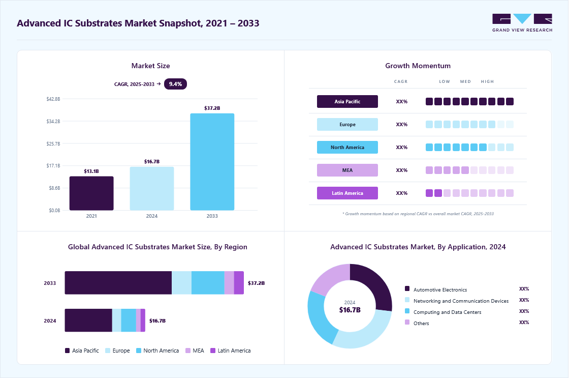
The global advanced IC substrates market size was estimated at USD 16.73 billion in 2024, and is projected to reach USD 37.20 billion by 2033, growing at a CAGR of 9.4% from 2025 to 2033. The rising adoption of heterogeneous integration and chiplet-based architectures has emerged as a significant trend in the global advanced IC substrates industry, driving demand for high-density.
Key Market Trends & Insights
- The Asia Pacific advanced IC substrates market accounted for a 58.9% revenue share in 2024.
- The advanced IC substrates industry in China held a dominant position in 2024.
- By type, the flip chip ball grid array substrates segment accounted for the largest share of 36.5% in 2024.
- By technology, the high-density interconnect substrates segment held the largest market share in 2024.
- By application, the mobile and consumer electronics segment dominated the market in 2024.
Market Size & Forecast
- 2024 Market Size: USD 16.73 Billion
- 2033 Projected Market Size: USD 37.20 Billion
- CAGR (2025-2033): 9.4%
- Asia Pacific: Largest market in 2024
These multi-layer substrates enable compact, energy-efficient, and high-performance semiconductor packaging across AI, 5G, and automotive applications. The global push toward electric mobility and cleaner transportation is significantly boosting the demand for advanced IC substrates. The adoption of wide bandgap semiconductors such as silicon carbide and gallium nitride is becoming central to electric vehicle powertrains and high-voltage industrial systems. Silicon carbide has gained widespread traction since its use in electric vehicle inverters by major manufacturers like Tesla. Its superior properties, such as higher electric field tolerance and thermal conductivity, make it ideal for demanding automotive environments. This shift is further supported by projections that semiconductors will account for over 20 percent of a premium vehicle’s total value by 2030, up from just four percent in 2019. As a result, demand for robust substrate materials that support high voltage and temperature performance is propelling the market growth in the automotive sector.The surge in artificial intelligence applications is reshaping the semiconductor landscape, placing intense performance demands on packaging and substrate technologies. AI chips now require rapid data transfer, lower power consumption, and enhanced thermal performance, which is pushing the industry to develop more sophisticated packaging solutions. The National Advanced Packaging Manufacturing Program has identified artificial intelligence as a key driver requiring innovation in equipment, power delivery, and chiplet support systems. Government-backed investments are accelerating research in these areas, with expectations of one hundred million dollars in funding over the next five years. These developments are boosting the demand for high-density and thermally efficient substrates, particularly those optimized for AI-centric hardware in data centers and edge devices, thereby propelling the overall market growth.
")
The semiconductor industry is undergoing a major transformation as it shifts toward heterogeneous integration and chiplet-based system architectures. Traditional monolithic chip designs are being replaced with modular chiplet configurations that improve yield and lower costs. This evolution requires advanced IC substrates to serve as the high-performance interconnect platform supporting seamless communication between diverse chiplets. Research forecasts indicate that the future of packaging will move toward simplified hierarchy with direct chiplet-to-substrate assembly, replacing the need for intermediary layers like interposers. Substrate technologies are being adapted to include silicon and glass cores, along with embedded passive and active components. This architectural shift is boosting the market by enabling more efficient, scalable, and cost-effective semiconductor design and manufacturing.
The transition from round wafer-based processing to large area panel-level packaging is redefining the substrate manufacturing process. Panel sizes reaching up to six hundred fifty millimeters by six hundred fifty millimeters are enabling manufacturers to process more devices per cycle, significantly improving throughput and lowering production costs. This evolution is particularly impactful for high-volume sectors such as mobile electronics, medical wearables, and flexible hybrid devices. The use of larger panels also allows for the integration of more complex designs on thinner substrates, expanding the range of potential applications.
In response to recent supply chain disruptions, several governments are focusing on reshoring and domesticating the production of advanced IC substrates. The U.S. currently has minimal capacity to manufacture high-end substrates like Flip Chip Ball Grid Array or Flip Chip Chip Scale Package, which are critical to leading-edge chip packaging. As part of the CHIPS and Science Act, federal support totaling nearly three hundred million dollars is being directed toward building domestic capabilities. These efforts include investment in emerging technologies such as additive manufacturing and three-dimensional printing for substrate prototyping. The aim is to reduce dependence on foreign suppliers and establish a more resilient and secure supply network for the semiconductor industry. These strategic moves are boosting the market by ensuring consistent access to advanced packaging technologies and driving long-term growth across key verticals.
Type Insights
The Flip Chip Ball Grid Array (FCBGA) Substrates segment accounted for the largest share of 36.5% in 2024. The increasing integration of AI accelerators and high-speed interfaces in data center processors has triggered a significant shift toward ultra-large FCBGA substrates, which offer improved electrical performance and thermal dissipation. This trend is being fueled by hyperscale cloud providers and chipmakers seeking substrates that can handle chiplet-based packages, leading to a sustained surge in demand for FCBGA in server and networking applications.
The embedded substrates segment is projected to grow at the fastest CAGR over the forecast period. The surge in edge AI and wearable medical devices is driving a unique demand for ultra-miniaturized embedded substrates that integrate passive and active components within the substrate layer itself. Unlike conventional substrates, this technology enables thinner profiles and shorter interconnect paths, making it ideal for space-constrained and performance-critical applications such as neural monitoring headbands and AR glasses.
Technology Insights
The High-Density Interconnect (HDI) Substrates segment held the largest share of the advanced IC substrates market in 2024. As smartphone makers race to embed advanced biometric and AI features in slimmer form factors, HDI substrates have emerged as the backbone of multi-functional SoCs. The shift toward triple-stacked camera modules, in-screen fingerprint sensors, and multi-band RF units is compelling substrate manufacturers to innovate with finer line/space geometries and advanced via stacking, propelling growth in the HDI segment.
The coreless substrates segment is projected to grow at the fastest CAGR over the forecast period. The evolution of next-gen mobile processors with ultra-high I/O density and higher frequency operation has accelerated the adoption of coreless substrates. Their ability to reduce warpage and improve signal integrity at sub-10nm node packaging is turning coreless substrates into a preferred solution for premium smartphones and foldable devices, especially in flagship-level SoCs from leading OEMs.
Application Insights
The mobile and consumer electronics segment dominated the advanced IC substrates industry in 2024 and is projected to grow at a significant CAGR over the forecast period. The rising use of multi-chip packaging for advanced camera AI, real-time language processing, and on-device security is reshaping substrate requirements in mobile and consumer electronics. This shift is generating demand for versatile substrates capable of supporting mixed-signal, logic, and memory integration on a single package, especially as foldable, wearable, and satellite-connected phones become mainstream.

The automotive electronics segment is projected to grow at the fastest CAGR over the forecast period. The transition to software-defined vehicles and zone-based E/E architectures is creating new pressure on substrate technologies to deliver automotive-grade reliability at higher data bandwidths. With ADAS, in-vehicle infotainment, and power electronics converging into centralized modules, the demand for high-reliability IC substrates, especially those supporting high-voltage and thermal resilience, is accelerating rapidly across EV platforms.
Regional Insights
The North America advanced IC substrates market accounted for 18.7% share of the overall market in 2024. The market growth is significantly driven by strong governmental backing through the CHIPS and Science Act. The U.S. government has allocated substantial funding, over USD 50 billion in total, with around USD 300 million specifically aimed at enhancing advanced packaging and substrate capabilities. More recently, a USD 1.6 billion fund was announced to expand packaging infrastructure, particularly focused on Flip Chip Ball Grid Array (FCBGA) and Flip Chip Chip Scale Package (FCCSP) substrates. These initiatives are not only attracting investments from leading industry players such as AMD, Nvidia, and Apple, but are also helping reduce reliance on foreign supply chains. As a result, these efforts are steadily boosting North America’s substrate manufacturing capacity and are expected to propel growth in sectors like artificial intelligence, telecommunications, and high-performance computing.
U.S. Advanced IC Substrates Industry Trends
The U.S. advanced IC substrates industry held a dominant position in 2024.The Department of Energy states that wide bandgap semiconductors like SiC and GaN are expected to make up nearly 20% of the power device market share by 2026, specifically around 14% for SiC and 5% for GaN . As EVs and industrial high-voltage systems deploy these technologies, demand for specialized substrates capable of handling high thermal loads and voltage stress is driving advanced IC substrate adoption across U.S.-based manufacturers.
Europe Advanced IC Substrates Market Trends
Europe holds a substantial share of the advanced IC substrates industry. In Europe, the regional market is being strengthened through the European Chips Act, which mobilizes more than €43 billion in combined public and private investments to be deployed by 2030. A critical component of this effort is the establishment of local semiconductor packaging and substrate fabrication capacity, which aims to double the EU's global semiconductor production share from 10% to 20%. These programs prioritize the development of high-density interconnect substrates and technologies that support heterogeneous integration. By funding pilot projects and encouraging innovation in substrate design and fabrication, Europe is laying the groundwork for long-term strategic autonomy. It is creating an environment that supports the growth of advanced IC substrate demand across the automotive, defense, and consumer electronics sectors.
The Germany advanced IC substrates market is expected to grow over the forecast period. Germany’s Federal Ministry of Education and Research (BMBF) has funded multiple public-private partnerships in advanced packaging R&D, focusing on high-density interconnect substrates for automotive electronics. These initiatives align with Germany’s leadership in EV and ADAS deployment and are boosting advanced IC substrate demand in its automotive sector.
The advanced IC substrates market in the UK is projected to grow during the forecast period. The UK government’s 2021 National Semiconductor Strategy commits to supporting advanced packaging and substrate capabilities, with a focus on AI, defense, and 5G infrastructure. This strategy includes grants and matched funding to encourage FCBGA and other substrate lines, propelling the local advanced IC substrate ecosystem.
Asia Pacific Advanced IC Substrates Market Trends
Asia Pacific continues to lead the global advanced IC substrates industry, fueled by aggressive government strategies across key economies such as China, Japan, and India. China’s 14th Five-Year Plan has elevated semiconductors to a national priority, channeling funding into substrate R&D and fabrication, particularly for FCBGA and HDI technologies. Japan’s Society 5.0 program, meanwhile, encourages public-private collaboration in advanced electronics manufacturing, with an emphasis on materials like silicon carbide and gallium nitride for use in power and automotive electronics. India is also entering the race with its National Semiconductor Mission, which includes support for packaging and substrate infrastructure development. Collectively, these national strategies are expanding local manufacturing ecosystems and significantly boosting the region’s dominance in substrate production and innovation, propelling long-term growth in advanced electronics manufacturing.

The China advanced IC substrates market is anticipated to grow over the forecast period. China’s “14th Five-Year Plan for the Integrated Circuit Industry” allocates significant capital to advanced packaging, including substrate R&D and production. This commitment supports national substrate champions in scaling FCBGA, HDI, and embedded packaging, boosting China’s domestic substrate capabilities.
The advanced IC substrates market in Japan is expected to witness growth over the forecast period. Japan’s National Strategic Special Zones and “Society 5.0” vision include cooperation grants for advanced semiconductor packaging, specifically targeting high-reliability substrates for automotive and industrial applications. These programs are driving substrate technology deployment in mission-critical sectors.
The India advanced IC substrates market is expected to grow during the forecast period. India’s 2023 National Semiconductor Mission (through MeitY) includes a standalone pillar for semiconductor assembly, packaging, and testing infrastructure, with substrate capacity being a key component. Public investment and incentives are being used to boost domestic substrate manufacturing and reduce reliance on imports.
Key Advanced IC Substrates Company Insights
Some of the major players in the advanced IC substrates market include ASE TECHNOLOGY HOLDING, AT&S Austria Technologie & Systemtechnik Aktiengesellschaft, Fujitsu, IBIDEN, and KINSUS INTERCONNECT TECHNOLOGY CORP., due to their expansive manufacturing capacities, consistent investments in next-generation packaging technologies, and strong partnerships with top-tier semiconductor and electronics companies. These firms have demonstrated excellence in producing high-performance substrates used in cutting-edge applications such as artificial intelligence, 5G communication, high-performance computing, and automotive electronics. Their ability to support technologies like flip chip ball grid arrays, high-density interconnects, coreless designs, and embedded substrates makes them critical to the value chain. Additionally, their strategic global footprint, integration of sustainable practices, and focus on R&D-driven innovation continue to boost their relevance and competitiveness in this rapidly evolving market.
-
ASE Technology Holding is one of the world's largest providers of semiconductor manufacturing services in assembly and testing. The company plays a leading role in the advanced IC substrates industry through its robust capabilities in flip chip, system-in-package (SiP), and high-density interconnect technologies. ASE offers a comprehensive portfolio of substrate-based packaging solutions, including Flip Chip Ball Grid Array (FCBGA) and Embedded Substrate technologies, tailored for high-performance computing, mobile, automotive, and networking applications. Its global scale and deep expertise position it as a key enabler of complex, multi-die integration and heterogeneous chip architectures.
-
AT&S Austria Technologie & Systemtechnik Aktiengesellschaft is a globally recognized manufacturer of high-end printed circuit boards and IC substrates. The company specializes in producing advanced substrate technologies used in flip chip packaging and high-frequency applications. With a strong focus on R&D, AT&S has become a preferred supplier to leading semiconductor and electronics companies, offering solutions that support miniaturization, signal integrity, and thermal performance in advanced processors. Its manufacturing expertise spans High-Density Interconnect (HDI), coreless, and build-up substrates, serving demanding markets such as mobile devices, automotive electronics, medical technology, and data centers.
Key Advanced IC Substrates Companies:
The following are the leading companies in the advanced IC substrates market. These companies collectively hold the largest market share and dictate industry trends.
- ASE TECHNOLOGY HOLDING
- AT&S Austria Technologie & Systemtechnik Aktiengesellschaft
- Fujitsu
- IBIDEN
- KINSUS INTERCONNECT TECHNOLOGY CORP
- KYOCERA Corporation
- LG Innotek
- NAN YA PLASTICS CORPORATION
- SAMSUNG ELECTRO-MECHANICS
- Unimicron
Recent Developments
-
In March 2025, AT&S secured a USD250 million sustainability-linked loan from the International Finance Corporation (IFC), a World Bank Group institution, to support the development of its modern IC substrate plant in Kulim, Malaysia. The loan is linked to AT&S, reducing annual greenhouse gas emissions by 31% by fiscal year 2028 compared to its 2022 baseline. This financing aims to expand production for AMD’s data‑center processors, thereby boosting substrate manufacturing capacity in Southeast Asia.
-
In February 2025, ASE Group inaugurated its fifth chip packaging and testing facility in Penang, Malaysia. This new plant expanded its footprint to 3.4 million square feet. It introduced AIoT-driven automation for yield optimization and environmental sensing, reinforcing ASE’s global capacity to support GenAI, EV, and autonomous driving chip packaging.
Advanced IC Substrates Market Report Scope
Report Attribute
Details
Market size value in 2025
USD 18.13 billion
Revenue forecast in 2033
USD 37.20 billion
Growth rate
CAGR of 9.4% from 2025 to 2033
Base year for estimation
2024
Historical data
2021 - 2023
Forecast period
2025 - 2033
Quantitative units
Revenue in USD million/billion and CAGR from 2025 to 2033
Report coverage
Revenue forecast, company ranking, competitive landscape, growth factors, and trends
Segments covered
Type, technology, application, region
Regional scope
North America; Europe; Asia Pacific; Latin America; MEA
Country scope
U.S.; Canada; Mexico; Germany; UK; France; China; Japan; India; South Korea; Australia; Brazil; KSA; UAE; South Africa
Key companies profiled
ASE TECHNOLOGY HOLDING; AT&S Austria Technologie & Systemtechnik Aktiengesellschaft; Fujitsu; IBIDEN; KINSUS INTERCONNECT TECHNOLOGY CORP; KYOCERA Corporation; LG Innotek; NAN YA PLASTICS CORPORATION; SAMSUNG ELECTRO-MECHANICS; Unimicron
Customization scope
Free report customization (equivalent up to 8 analysts working days) with purchase. Addition or alteration to country, regional & segment scope.
Pricing and purchase options
Avail customized purchase options to meet your exact research needs. Explore purchase options
Global Advanced IC Substrates Market Report Segmentation
This report forecasts revenue growth at the global, regional, and country levels and provides an analysis of the latest industry trends in each of the sub-segments from 2021 to 2033. For this study, Grand View Research has segmented the global advanced IC substrates market report based on type, technology, application, and region:

-
Type Outlook (Revenue, USD Million, 2021 - 2033)
-
Flip Chip Ball Grid Array (FCBGA) Substrates
-
Flip Chip Chip Scale Package (FCCSP) Substrates
-
Wire Bond Substrates
-
Embedded Substrates
-
Others
-
-
Technology Outlook (Revenue, USD Million, 2021 - 2033)
-
High-Density Interconnect (HDI) Substrates
-
Build-Up Substrates
-
Coreless Substrates
-
Organic Substrates
-
Ceramic Substrates
-
-
Application Outlook (Revenue, USD Million, 2021 - 2033)
-
Mobile and Consumer Electronics
-
Automotive Electronics
-
Networking and Communication Devices
-
Computing and Data Centers
-
Others
-
-
Regional Outlook (Revenue, USD Million, 2021 - 2033)
-
North America
-
U.S.
-
Canada
-
Mexico
-
-
Europe
-
Germany
-
UK
-
France
-
-
Asia Pacific
-
China
-
Japan
-
India
-
South Korea
-
Australia
-
-
Latin America
-
Brazil
-
-
Middle East and Africa (MEA)
-
KSA
-
UAE
-
South Africa
-
-
Frequently Asked Questions About This Report
The global advanced IC substrates market size was estimated at USD 16.73 billion in 2024 and is expected to reach USD 18.13 billion in 2025.
The global advanced IC substrates market size is expected to grow at a significant CAGR of 9.4% to reach USD 37.20 billion in 2033.
Asia Pacific held the largest market share of 58.9% in 2024, fueled by aggressive government strategies across key economies such as China, Japan, and India. China’s 14th Five-Year Plan has elevated semiconductors to a national priority, channeling funding into substrate R&D and fabrication, particularly for FCBGA and HDI technologies.
Some of the players in the advanced IC substrates market are ASE TECHNOLOGY HOLDING, AT&S Austria Technologie & Systemtechnik Aktiengesellschaft, Fujitsu, IBIDEN, KINSUS INTERCONNECT TECHNOLOGY CORP, KYOCERA Corporation, LG Innotek, NAN YA PLASTICS CORPORATION, SAMSUNG ELECTRO-MECHANICS, and Unimicron.
The key driving trend in the advanced IC substrates market is the surging demand for high-density, miniaturized packaging technologies to support cutting‑edge applications like AI, 5G, HPC, and automotive electronics, leading to innovations such as advanced packaging, heterogeneous integration, HDI, and glass-core substrates.
About the Author(s)
Semiconductors Research Team
Semiconductors & Electronics · SemiconductorsThis report was authored by the semiconductors research team at Grand View Research - comprising two research analysts, one senior research analyst, and one industry expert - with specialized expertise in the semiconductors segment of the semiconductors & electronics industry. All findings are based on proprietary semiconductors & electronics databases, executive interviews, and regulatory analysis, subject to internal peer review prior to publication.
Last Updated:
Speak to Analyst


Need a Tailored Report?
Customize this report to your needs — add regions, segments, or data points, with 20% free customization.
Or view our licence options:

ISO 9001:2015 & 27001:2022 Certified
We are GDPR and CCPA compliant! Your transaction & personal information is safe and secure. For more details, please read our privacy policy.