
- Home
- »
- Advanced Interior Materials
- »
-
Extreme Ultraviolet Lithography Market Report, 2026-2033GVR Report cover

Extreme Ultraviolet Lithography Market (2026 - 2033)
Size, Share & Trends Analysis Report By Equipment (Light Source, Optics, Mask), By End Use (Integrated Device Manufacturer, Foundries), By Region (North America, Europe, Asia Pacific), And Segment Forecasts
Market Size, 2025
$11.3BMarket Estimate, 2026
$12.6BMarket Forecast, 2033
$37.2BCAGR, 2026–2033
16.8%Extreme Ultraviolet Lithography Market Summary
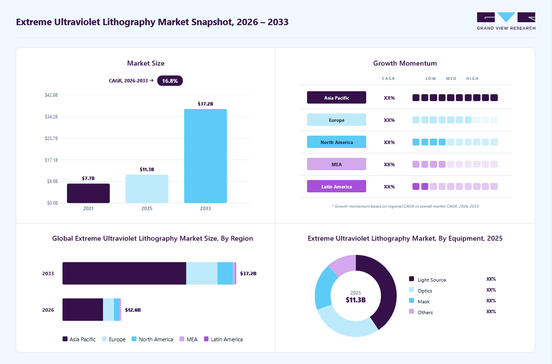
The global extreme ultraviolet lithography market size was valued at USD 11.3 billion in 2025 and is projected to grow from USD 12.6 billion in 2026 to USD 37.2 billion by 2033, at a CAGR of 16.8% from 2026 to 2033. Asia Pacific dominated the market, accounting for a revenue share of 69.0% in 2025. The EUV lithography market is experiencing robust growth driven by the rising demand for smaller and more efficient semiconductor devices.
 Source: Grand View Research, IR Documents, Primary Interviews, Paid DatabasesTo learn more about this report,
 Download Free Sample Report
Key Market Trends & Insights
- By equipment: Light source segment dominated the market, with a revenue share of 40.5% in 2025.
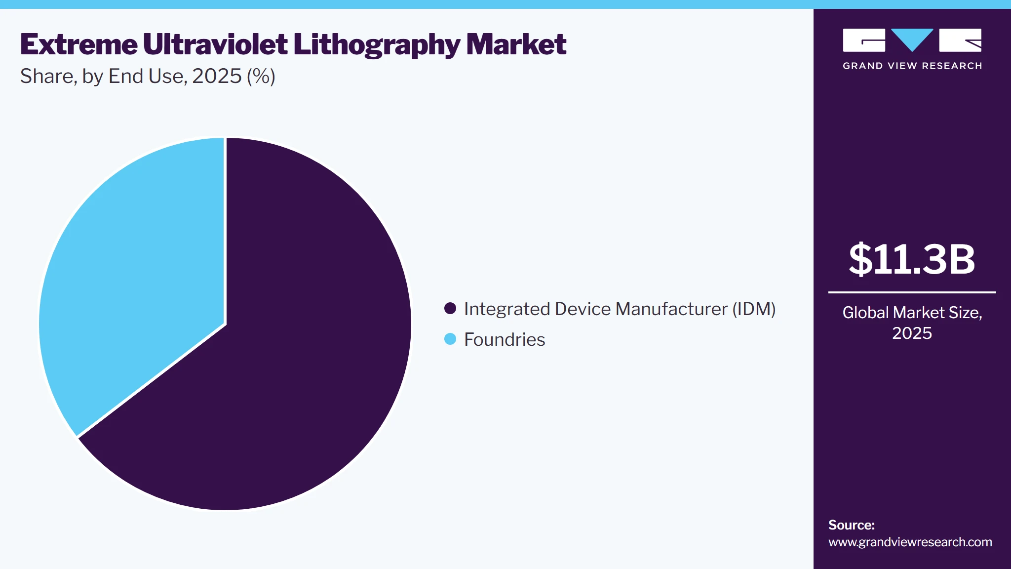
- By end use: Integrated device manufacturer (IDM) segment held the largest market share of 64.6% in 2025.
Regional Highlights
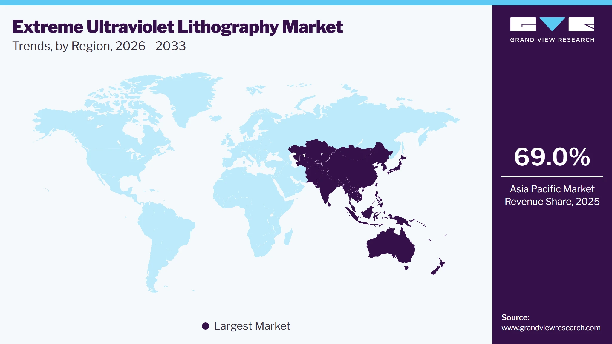
- Largest regional market: Asia Pacific (69.0% revenue share, 2025)
- By country: The U.S. held the largest market share in 2025.
Market Size & Forecast
- Market size in 2025: USD 11.3 Billion
- Estimated market size in 2026: USD 12.6 Billion
- Projected market size by 2033: USD 37.2 Billion
- CAGR (2026-2033): 16.8%
Three ways to get this report
Buy it, customize it, or ask a question.Ask an Analyst
Analyst response in 1 business day
- AccessReport author, directly
- Reply timeWithin 1 working day
- No sales callDirect answer only
- FormatEmail reply
- CostFree, no cost
Get the Full Report
What the study covers
- FormatsPDF · Excel · Dashboard
- Timeline2026–2033 annual, 2025 base
- Coverage20+ countries, 5 regions
- Companies10+ key players profiled
Customize the Report
20% free customization
- IncludeCountries, segments, points
- TailorTo your product definition
- ExtendDeeper competitor detail
- OrA fully bespoke study
- Turnaround5–10 working days
As electronics continue to shrink while simultaneously increasing in power and efficiency, manufacturers are turning to extreme ultraviolet (EUV) lithography as a key technology to produce the next generation of semiconductors. This trend is primarily fueled by the ongoing advancements in sectors such as consumer electronics, automotive, and high-performance computing. The EUV lithography is a cutting-edge technology used in the semiconductor manufacturing process to create highly intricate patterns on silicon wafers. This technology employs extremely short wavelengths of light, in the extreme ultraviolet spectrum, to achieve unprecedented resolutions and precision, enabling the production of semiconductor devices that are smaller, faster, and more efficient. EUV lithography represents a significant advancement over traditional lithography techniques, opening the door to the next generation of microchips required for various high-tech applications, from smartphones and computers to advanced AI and 5G networks.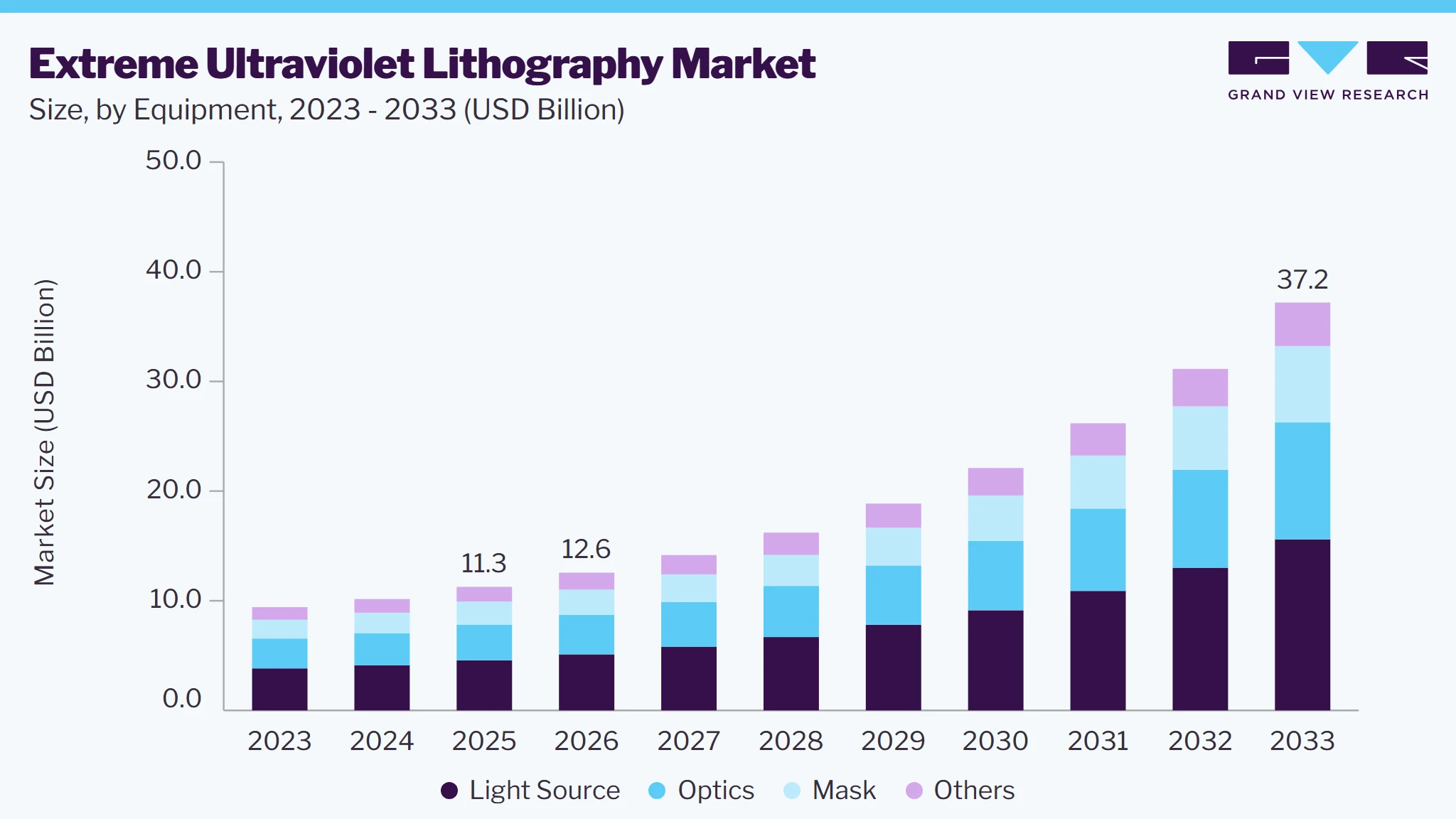 To learn more about this report, Download Free Sample Report
Another factor contributing to the growth of the EUV lithography market is the rapid pace of innovation and technological advancements within the semiconductor industry itself. As chip manufacturers continue to push the boundaries of what's possible, EUV lithography stands out as a critical tool for realizing these advancements, thanks to its unparalleled precision and scalability.
Market Dynamics
The extreme ultraviolet (EUV) lithography market is influenced by continuous advancements in semiconductor process technologies, increasing demand for smaller and higher-performance chips, expanding investments in advanced wafer fabrication facilities, and the industry's transition toward sub-5 nm and next-generation process nodes. Ongoing improvements in EUV light source power, photomask technology, photoresists, and High-NA EUV systems are enhancing manufacturing precision and production efficiency. At the same time, stringent cleanroom requirements, complex system integration, limited supplier availability for critical components, high capital expenditure, extended equipment lead times, and geopolitical factors affecting semiconductor manufacturing and supply chains continue to shape production strategies, technology adoption, and competitive dynamics across the market.
The increasing demand for high-performance processors, AI accelerators, advanced memory, and mobile chipsets is driving the adoption of extreme ultraviolet lithography. Semiconductor manufacturers are transitioning to smaller technology nodes such as 5 nm, 3 nm, and below to improve transistor density, power efficiency, and processing performance. EUV lithography enables precise patterning with fewer processing steps compared to conventional lithography techniques, helping manufacturers improve yield and production efficiency. Continued investments in advanced semiconductor fabrication facilities by leading foundries and integrated device manufacturers are further strengthening demand for EUV lithography systems.
The adoption of EUV lithography is constrained by the substantial investment required for equipment, supporting infrastructure, and specialized manufacturing environments. EUV systems involve highly sophisticated optics, light sources, masks, and contamination control technologies, making installation, operation, and maintenance technically demanding. Long equipment qualification cycles, limited manufacturing capacity for critical components, and the need for highly skilled personnel also increase implementation costs, limiting adoption primarily to large semiconductor manufacturers.
The development of High-Numerical Aperture (High-NA) EUV lithography is creating opportunities to support future semiconductor process nodes with improved resolution and patterning accuracy. At the same time, expanding investments in new wafer fabrication plants across Asia Pacific, North America, and Europe are increasing the deployment of advanced lithography equipment. Government initiatives to strengthen domestic semiconductor manufacturing, combined with growing demand for AI, high-performance computing, automotive electronics, and data center processors, are creating favorable conditions for the wider adoption of next-generation EUV lithography technologies.
Analyst Perspective
The extreme ultraviolet (EUV) lithography market is witnessing strong growth, driven by the transition to advanced semiconductor process nodes and rising demand for AI, high-performance computing (HPC), 5G, automotive electronics, and advanced memory devices. Increasing investments in semiconductor fabrication facilities, supported by government initiatives to strengthen domestic chip manufacturing, are accelerating the adoption of EUV lithography. Ongoing advancements in High-NA EUV technology, higher wafer throughput, and improved patterning precision are further enhancing manufacturing efficiency, positioning EUV systems for sustained long-term growth as chipmakers scale production of next-generation semiconductors.
Equipment Insights
Based on equipment, the light source segment led the market with the largest revenue share of 40.5% in 2025. The light source equipment segment in the extreme ultraviolet (EUV) lithography market is experiencing significant growth, primarily fueled by the semiconductor industry's push toward producing smaller, more efficient chips. This demand is driven by the critical role of EUV lithography in enabling the patterning of sub-10 nanometer features on silicon wafers, essential for next-generation semiconductor devices. Advancements in light source technology, substantial investments from leading semiconductor manufacturers, strategic partnerships for technological innovation, and government support for semiconductor research and development are key factors propelling this market segment.
The mask equipment segment plays a crucial role in the EUV lithography market, exhibiting substantial growth as the demand for advanced semiconductor devices escalates. With EUV lithography enabling the production of chips at sub-7 nanometer geometries, the complexity and precision required in mask making have significantly increased. Masks, or photomasks, are essential for transferring circuit patterns onto semiconductor wafers, and the precision of this process directly influences the performance and yield of the final semiconductor products. The above factors will further drive the demand for extreme ultraviolet (EUV) lithography.
End Use Insights
Based on end use, the integrated device manufacturer (IDM) segment led the market with the largest revenue share of 64.6% in 2025. IDMs company which engages in the design, manufacture, and sales semiconductor products, are increasingly adopting EUV lithography to push the boundaries of chip performance, power, and area (PPA). This adoption is driven by the escalating demand for more powerful and efficient electronic devices across various applications, including computing, mobile, automotive, and IoT. Moreover, EUV lithography, with its capability to pattern incredibly fine features onto silicon wafers, is crucial to produce next-generation semiconductor devices.
 To learn more about this report, Download Free Sample Report
The extreme ultraviolet (EUV) lithography market for foundries end use is poised for substantial growth, given its critical role in propelling semiconductor manufacturing to new heights. As the semiconductor industry continues its relentless drive toward smaller, more powerful, and energy-efficient devices, foundries are increasingly relying on EUV lithography to meet these advanced technical requirements. This technology, renowned for its ability to pattern extremely fine features on silicon wafers, is vital for producing the next generation of semiconductor chips required for a multitude of applications, including smartphones, artificial intelligence, automotive, and high-performance computing.
Regional Insights
North America extreme ultraviolet (EUV) lithography market is significantly fuelled by the growing demand for smaller, more powerful semiconductor devices across a variety of industries, including computing, telecommunications, and consumer electronics. As the quest for miniaturization continues, with semiconductor manufacturers pushing the boundaries of Moore's Law, EUV lithography has emerged as a critical technology enabling the production of chips with feature sizes well below 10 nanometres, which is driving the expansion of the extreme ultraviolet (EUV) lithography market.
Asia Pacific Extreme Ultraviolet Lithography Market Trends
Asia Pacific dominated the extreme ultraviolet lithography market with the largest revenue share of 69.0% in 2025, primarily due to its robust semiconductor manufacturing base and the presence of leading semiconductor foundries. Countries like South Korea, Taiwan, and China are home to some of the world's largest semiconductor manufacturing companies and foundries, such as Samsung, TSMC, and SMIC, which are at the forefront of adopting cutting-edge manufacturing technologies, including EUV lithography. Which will drive the demand for extreme ultraviolet (EUV) lithography over the forecast period.
 To learn more about this report, Download Free Sample Report
China extreme ultraviolet lithography market is estimated to grow at a significant CAGR of 19.2’% over the forecast period. China's extreme ultraviolet (EUV) lithography market is experiencing rapid growth, driven by China’s increasing investments in research and development, as well as in the acquisition of state-of-the-art chipmaking equipment like EUV lithography systems. EUV lithography, critical for manufacturing next-generation semiconductor devices with smaller, more efficient circuits, is at the heart of China's strategy to excel in sectors such as 5G, artificial intelligence, and electric vehicles are key factors propelling the growth of the China EUV lithography market.
Taiwan Extreme Ultraviolet Lithography Market Trends
The extreme ultraviolet lithography market in Taiwan held the largest share in the Asia Pacific region in 2025. Taiwan extreme ultraviolet (EUV) lithography market is expected to witness growth driven by the country's strong semiconductor manufacturing ecosystem, increasing investments in advanced process nodes, and rising demand for high-performance and energy-efficient chips. The growing adoption of EUV lithography for manufacturing advanced logic semiconductors, particularly at leading-edge nodes, is supporting demand for sophisticated lithography equipment, photoresists, masks, pellicles, and related process materials. Taiwan's leading foundries continue to invest in advanced fabrication facilities to support applications across artificial intelligence (AI), high-performance computing (HPC), smartphones, and data centers.
Europe Extreme Ultraviolet Lithography Market Trends
The extreme ultraviolet (EUV) lithography market in Europe is growing at a significant rate owing to advancements in semiconductor technology and a strong ecosystem of research and development. European semiconductor manufacturers and research institutions are heavily invested in leveraging EUV lithography to push the limits of chip miniaturization and performance key to staying competitive in the rapidly evolving tech landscape.
Key Extreme Ultraviolet Lithography Company Insights
Some of the key players operating in the market include ASML Holding NV, Intel Corporation, Samsung Electronics Co. Ltd among others.
-
ASML Holding NV specializes in developing complex machines that allow semiconductor manufacturers to create smaller, more powerful, and energy-efficient microchips, pivotal for driving technological innovation across various sectors. Its product portfolio includes deep ultraviolet (DUV) lithography machines and the groundbreaking extreme ultraviolet (EUV) lithography systems. ASML's EUV technology represents a significant leap forward in lithography, allowing chipmakers to etch patterns on silicon wafers at a large scale.
-
Intel Corporation is engaged in the development and manufacturing of microprocessors and semiconductor chips. As a critical supplier for personal computer manufacturers worldwide, Intel continues to shape the future of computing, artificial intelligence, and broadband digital communications through its relentless pursuit of technological advancement and a steadfast commitment to research and development. The company made a significant stride in the semiconductor industry with the adoption of extreme ultraviolet (EUV) lithography technology. This advancement allows for the creation of smaller, more efficient microprocessors by employing incredibly precise light sources to etch finer circuits on chips.
NTT Advanced Technology Corporation, Canon Inc. and Nikon Corporation, are some of the emerging market participants in the extreme ultraviolet (EUV) lithography market.
-
Nikon Corporation has diversified its portfolio to include a range of optical products, including microscopes, binoculars, and measurement instruments, showcasing its prowess in precision optics and imaging technology. The company's commitment to excellence and innovation has solidified its position in the market, allowing it to adapt to the rapidly changing technological landscape while continuing to inspire and empower visual storytelling through its advanced and user-friendly products. Company EUV products are capable of etching features on silicon wafers with unparalleled precision, supporting the semiconductor industry's relentless push toward miniaturization and the development of next-generation chips.
-
Canon Inc., a renowned global leader in imaging and optical products, has made significant strides in the semiconductor lithography equipment market with its entry into Extreme Ultraviolet (EUV) lithography technology. This move represents a pivotal advancement in chip manufacturing, allowing for more intricate and smaller microchip designs. EUV lithography stands out because it uses extremely short wavelengths, significantly improving the resolution and efficiency of the photolithography process, essential for producing next-generation semiconductor devices.
Key Extreme Ultraviolet Lithography Companies:
The following key companies have been profiled for this study on the extreme ultraviolet lithography market.
- ASML Holding NV
- NTT Advanced Technology Corporation
- Canon Inc
- Nikon Corporation
- Intel Corporation
- Taiwan Semiconductor Manufacturing Company Limited
- Samsung Electronics Co. Ltd
- Toppan Photomasks Inc
- ZEISS Group
- Ushio, Inc.
Competitive Benchmarking
Category
Operating Strategies
Competitive Edge
Weakness
Established Players (e.g., ASML Holding NV, Intel Corporation, and Samsung Electronics Co. Ltd.)
- These companies prioritize the development of high-precision lithography systems, advanced optics, and integrated semiconductor manufacturing solutions.
- They also expand service agreements, strengthen global support infrastructure, and collaborate with chipmakers for process optimization.
- Mature players possess strong technological expertise, extensive patent portfolios, and established relationships with leading semiconductor manufacturers.
- Their competitive advantage comes from advanced engineering capabilities, high-performance EUV systems, and integrated support services.
- Mature players face challenges related to extremely high research and development expenses, long product development cycles, and dependence on semiconductor industry investment trends.
- Complex manufacturing processes and reliance on specialized suppliers can create supply chain risks and production delays.
Emerging & Regional Players (e.g., NTT Advanced Technology Corporation, Canon Inc., and Nikon Corporation)
- Emerging players mainly focus on niche technology development, component innovation, and strategic collaborations with research institutions and semiconductor firms.
- These companies emphasize specialized solutions such as optical components, metrology systems, and semiconductor process enhancement technologies.
- Emerging players gain competitive advantage through technological flexibility, focused innovation, and faster adaptation to evolving semiconductor manufacturing requirements.
- Their smaller organizational structures support quicker decision-making and specialized product development.
- These emerging players often face limitations related to restricted financial resources, lower market recognition, and limited large-scale manufacturing capabilities.
- High entry barriers in the EUV lithography industry, including intellectual property restrictions and complex engineering requirements, can slow market penetration.
Recent Developments
- In January 2024, ZEISS Group introduced its High-NA (Numerical Aperture) Extreme Ultraviolet (EUV) lithography system. This cutting-edge system represents a monumental leap in semiconductor manufacturing, enabling the creation of microchips with incredibly fine features, compared to existing EUV systems.
Extreme Ultraviolet Lithography Market Report Scope
Report Attribute
Details
Market size in 2025
USD 11.3 billion
Estimated market size in 2026
USD 12.6 billion
Projected market size by 2033
USD 37.2 billion
Growth rate
CAGR of 16.8% from 2026 to 2033
Base year for estimation
2025
Historical data
2021 - 2024
Forecast period
2026 - 2033
Quantitative units
Revenue in USD billion and CAGR from 2026 to 2033
Report coverage
Revenue forecast, company ranking, competitive landscape, growth factors, and trends
Segments covered
Equipment, end use, region
Regional scope
North America; Europe; Asia Pacific; Latin America; Middle East & Africa
Country scope
U.S., Canada, Mexico, Germany, France, Italy, UK, Spain, China, Japan, India, South Korea, Taiwan, Brazil, Argentina, South Africa, Saudi Arabia, UAE
Key companies profiled
ASML Holding NV, NTT Advanced Technology Corporation, Canon Inc., Nikon Corporation, Intel Corporation, Taiwan Semiconductor Manufacturing Company Limited, Samsung Electronics Co. Ltd, Toppan Photomasks Inc, ZEISS Group, Ushio, Inc.
Customization scope
Free report customization (equivalent up to 8 analysts' working days) with purchase. Addition or alteration to country, regional & segment scope.
Pricing and purchase options
Avail customized purchase options to meet your exact research needs. Explore purchase options
Global Extreme Ultraviolet Lithography Market Report Segmentation
This report forecasts revenue growth at global, regional & country levels and provides an analysis on the industry trends in each of the sub-segments from 2021 to 2033. For this study, Grand View Research has segmented the global extreme ultraviolet lithography market report on the basis of equipment, end use, and region:
-
Equipment Outlook (Revenue, USD Million, 2021 - 2033)
-
Light Source
-
Optics
-
Mask
-
Others
-
-
End Use Outlook (Revenue, USD Million, 2021 - 2033)
-
Integrated Device Manufacturer (IDM)
-
Foundries
-
-
Regional Outlook (Revenue, USD Million, 2021 - 2033)
-
North America
-
U.S.
-
Canada
-
Mexico
-
-
Europe
-
UK
-
Germany
-
France
-
Italy
-
Spain
-
-
Asia Pacific
-
Japan
-
China
-
India
-
Taiwan
-
South Korea
-
-
Latin America
-
Brazil
-
Argentina
-
-
Middle East & Africa
-
South Africa
-
Saudi Arabia
-
UAE
-
-
Research Methodology
The extreme ultraviolet lithography Market figures in this report are based on a proven research process that combines executive interviews with secondary research from proprietary databases, company filings, and recognized regulatory and institutional sources. Market size is built through value-chain sizing - reconciling supply-side and demand-side estimates - and triangulated with bottom-up and top-down approaches. Every estimate passes multiple levels of expert validation before publication, with each extreme ultraviolet lithography segment quantified using the revenue-capture definitions in the table below.
Segment Definition
Segment - Equipment
Revenue Capture Definition
Light Source
Revenue is generated from the sale of EUV light source systems and related source modules that produce extreme ultraviolet radiation for semiconductor wafer patterning.
Optics
Revenue is generated from the sale of precision optical components, including reflective mirrors, projection optics, collector optics, and illumination systems used in EUV lithography equipment.
Mask
Revenue is generated from the sale of EUV photomasks, mask blanks, pellicles, and related mask technologies used for transferring circuit patterns onto semiconductor wafers.
Others
Revenue is generated from the sale of supporting EUV lithography equipment and components, including wafer stages, metrology modules, contamination control systems, vacuum subsystems, and other auxiliary technologies.
Segment - End Use
Revenue Capture Definition
Integrated Device Manufacturer (IDM)
Revenue is generated from the sale of EUV lithography equipment and related components to semiconductor companies that design and manufacture chips within their own fabrication facilities.
Foundries
Revenue is generated from the sale of EUV lithography equipment and related components to contract semiconductor manufacturers that fabricate chips for fabless companies and other customers.
Estimation Model
Layer Name
Key Question
Description
Semiconductor Manufacturing Demand Layer
Where is EUV lithography required?
Analyze demand across advanced semiconductor fabrication facilities producing logic devices, memory chips, processors, AI accelerators, and other high-performance integrated circuits. Assess wafer production capacity, technology node migration, and advanced chip manufacturing requirements to establish the addressable demand for EUV lithography systems.
Semiconductor Capacity Expansion Layer
Where is new equipment demand being created?
Evaluate investments in semiconductor fabrication plants, foundry expansions, memory manufacturing facilities, and advanced process technology development. Assess greenfield fabs, capacity additions, government semiconductor initiatives, and technology upgrades that drive procurement of new EUV lithography equipment.
Technology Adoption Layer
Which EUV lithography technologies are being deployed?
Segment demand by equipment type, light source, application, end use, and region. Apply adoption rates based on semiconductor process node, wafer size, production volume, throughput requirements, overlay accuracy, and resolution performance.
Revenue Generation Layer
How much market revenue is generated?
Estimate annual shipments of EUV lithography systems by equipment type, application, end-use industry, and region. Quantify revenues generated exclusively from the sale of new EUV lithography equipment supplied to semiconductor foundries, integrated device manufacturers (IDMs), and research institutions.
Delivered Customizations
This report has been delivered with the following In-depth customizations
Client Request
Customization Delivered
Value Adds
Competitive Benchmarking
Detailed benchmarking of key extreme ultraviolet lithography companies based on lithography technology capabilities, manufacturing footprint, global service network, research and development strength, and positioning across advanced semiconductor manufacturing applications. The study also assessed innovation in optics, light source systems, process control technologies, and semiconductor fabrication integration capabilities.
Provides a clearer understanding of technological leadership, product differentiation, and competitive positioning within the extreme ultraviolet lithography market. Helps identify partnership opportunities, technology development gaps, and strategic expansion priorities.
Regional Segmentation
Detailed regional segmentation assessed the market based on semiconductor manufacturing capabilities, advanced fabrication capacity, investments in wafer fabrication facilities, technology adoption levels, supply chain infrastructure, government policy support, research and development activities, and demand for advanced semiconductor devices across major global regions.
Helps stakeholders identify high-growth regions, evaluate investment opportunities, understand regional demand and manufacturing trends, assess supply chain strengths, and develop region-specific market entry and expansion strategies.
Opportunity assessment
Identification of growth opportunities linked to rising semiconductor demand for artificial intelligence, 5G infrastructure, high-performance computing, advanced consumer electronics, and automotive electronics. The study also evaluated opportunities in sub-5 nm chip manufacturing, advanced semiconductor fabrication facilities, precision optics development, and next-generation lithography technologies supporting advanced chip production.
Helps companies align long-term growth strategies with semiconductor technology advancements, increasing chip production investments, and demand for advanced lithography infrastructure. Supports investment planning and market expansion strategies.
Frequently Asked Questions About This Report
The global extreme ultraviolet lithography market size was valued at USD 11.3 billion in 2025 and is estimated at USD 12.6 billion in 2026.
The global extreme ultraviolet lithography market is expected to grow at a CAGR of 16.8% from 2026 to 2033, reaching USD 37.2 billion by 2033.
Asia Pacific dominated with a 69.0% revenue share in 2025.
Key players include ASML Holding NV, NTT Advanced Technology Corporation, Canon Inc., Nikon Corporation, Intel Corporation, Taiwan Semiconductor Manufacturing Company Limited, Samsung Electronics Co. Ltd, Toppan Photomasks Inc, ZEISS Group, Ushio, Inc.
The light source segment led the market with the largest revenue share of 40.5% in 2025.The light source equipment segment in the extreme ultraviolet (EUV) lithography market is experiencing significant growth, primarily fueled by the semiconductor industry's push toward producing smaller, more efficient chips.
The integrated device manufacturer (IDM) segment dominated for the largest revenue share of 64.6% in 2025.
The extreme ultraviolet (EUV) lithography market is experiencing robust growth driven by the escalating demand for smaller, more efficient semiconductor devices. As electronics continue to shrink while simultaneously increasing in power and efficiency, manufacturers are turning to extreme ultraviolet (EUV) lithography as a key technology to produce the next generation of semiconductors. This trend is primarily fueled by the ongoing advancements in sectors such as consumer electronics, automotive, and high-performance computing.
About the Author(s)
Advanced Interior Materials Research Team
Advanced Materials · Advanced Interior MaterialsThis report was authored by the advanced interior materials research team at Grand View Research - comprising two research analysts, one senior research analyst, and one industry expert - with specialized expertise in the advanced interior materials segment of the advanced materials industry. All findings are based on proprietary advanced materials databases, executive interviews, and regulatory analysis, subject to internal peer review prior to publication.
Last Updated:
Speak to Analyst

Customize this report to your needs - add regions, segments, or data points, with 20% free customization.
Or view our licence options:


ISO 9001:2015 & 27001:2022 Certified
We are GDPR and CCPA compliant! Your transaction & personal information is safe and secure. For more details, please read our privacy policy.


