
- Home
- »
- Advanced Interior Materials
- »
-
Failure Analysis Test Equipment for Semiconductors Market Report 2033GVR Report cover

Failure Analysis Test Equipment For Semiconductors Market (2026 - 2033)
Size, Share & Trends Analysis Report By Product (Scanning Electron Microscope, Transmission Electron Microscope, Focused Ion Beam System), By Technology, By Region, And Segment Forecasts
Market Size, 2025
$2.4BMarket Estimate, 2026
$2.6BMarket Forecast, 2033
$4.5BCAGR, 2026–2033
8.6%Market Size & Trends
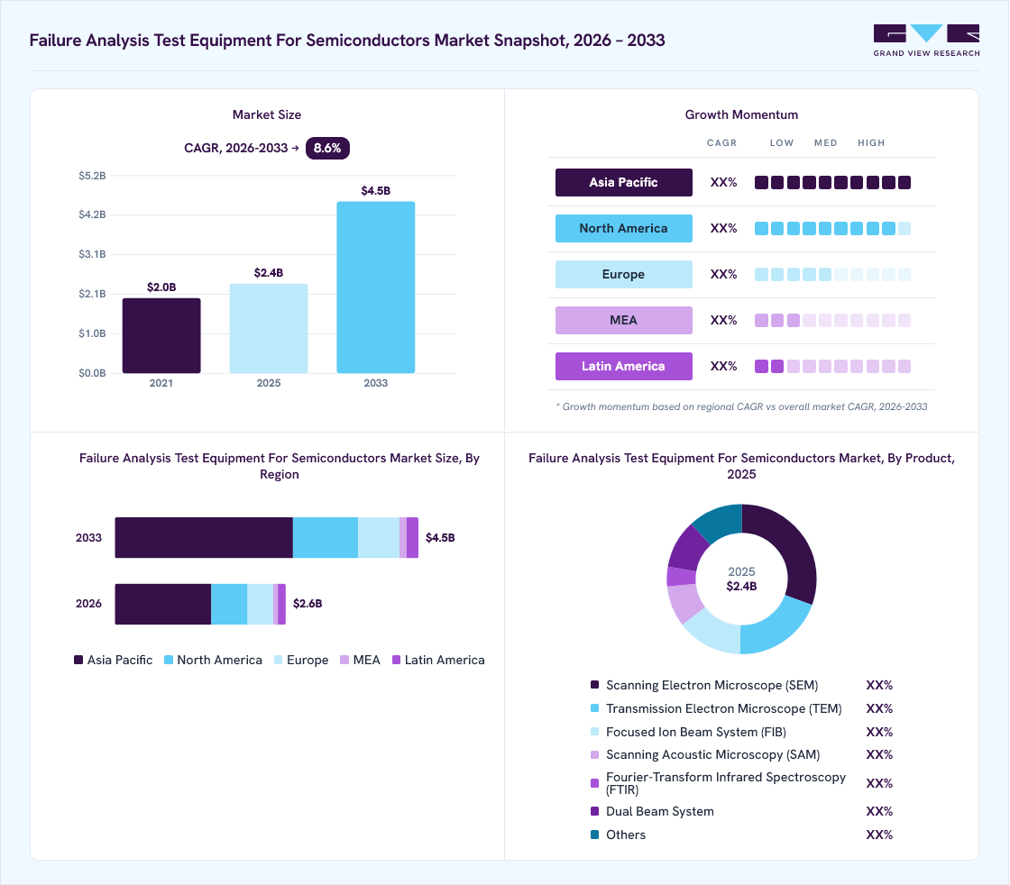
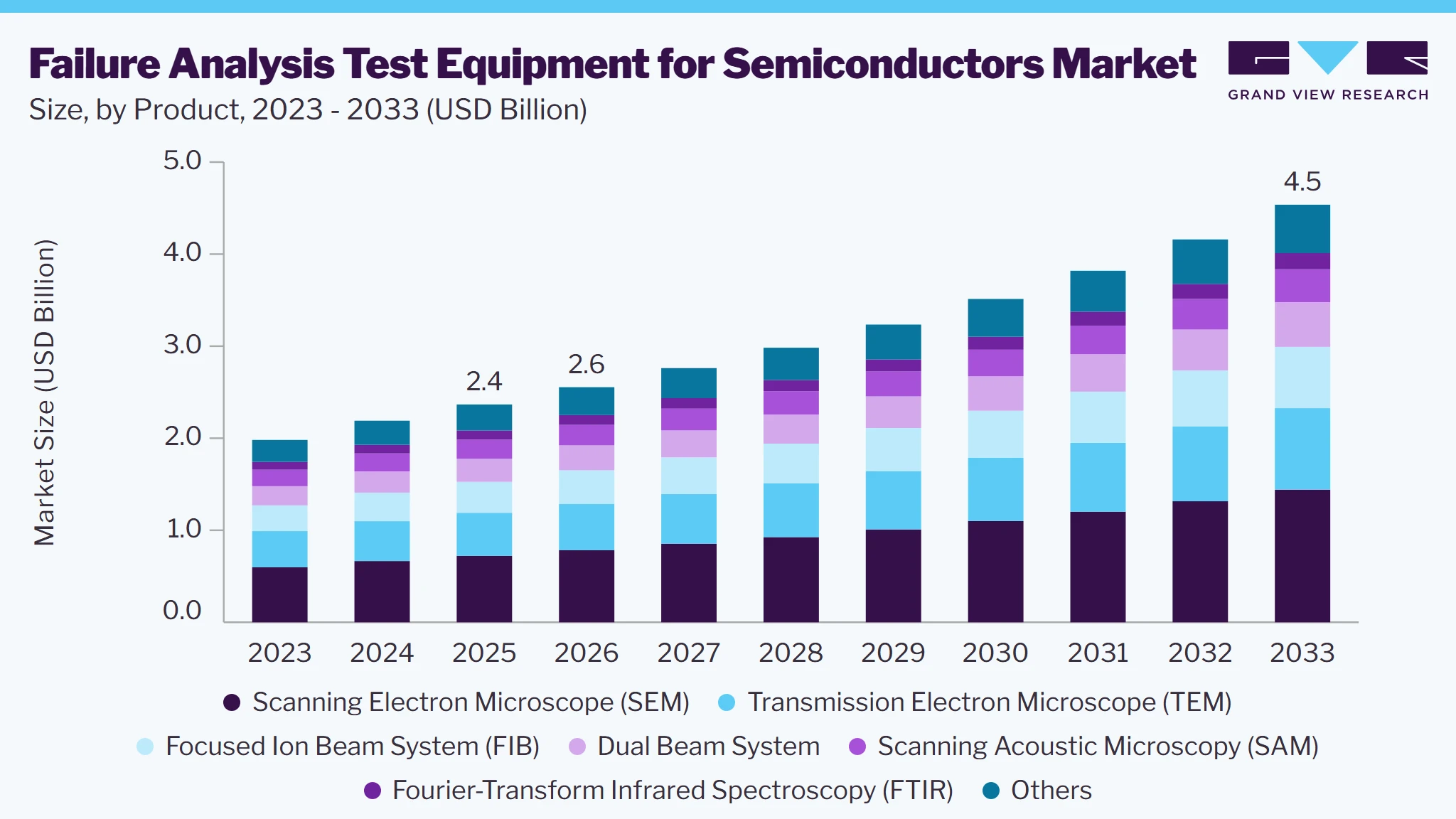
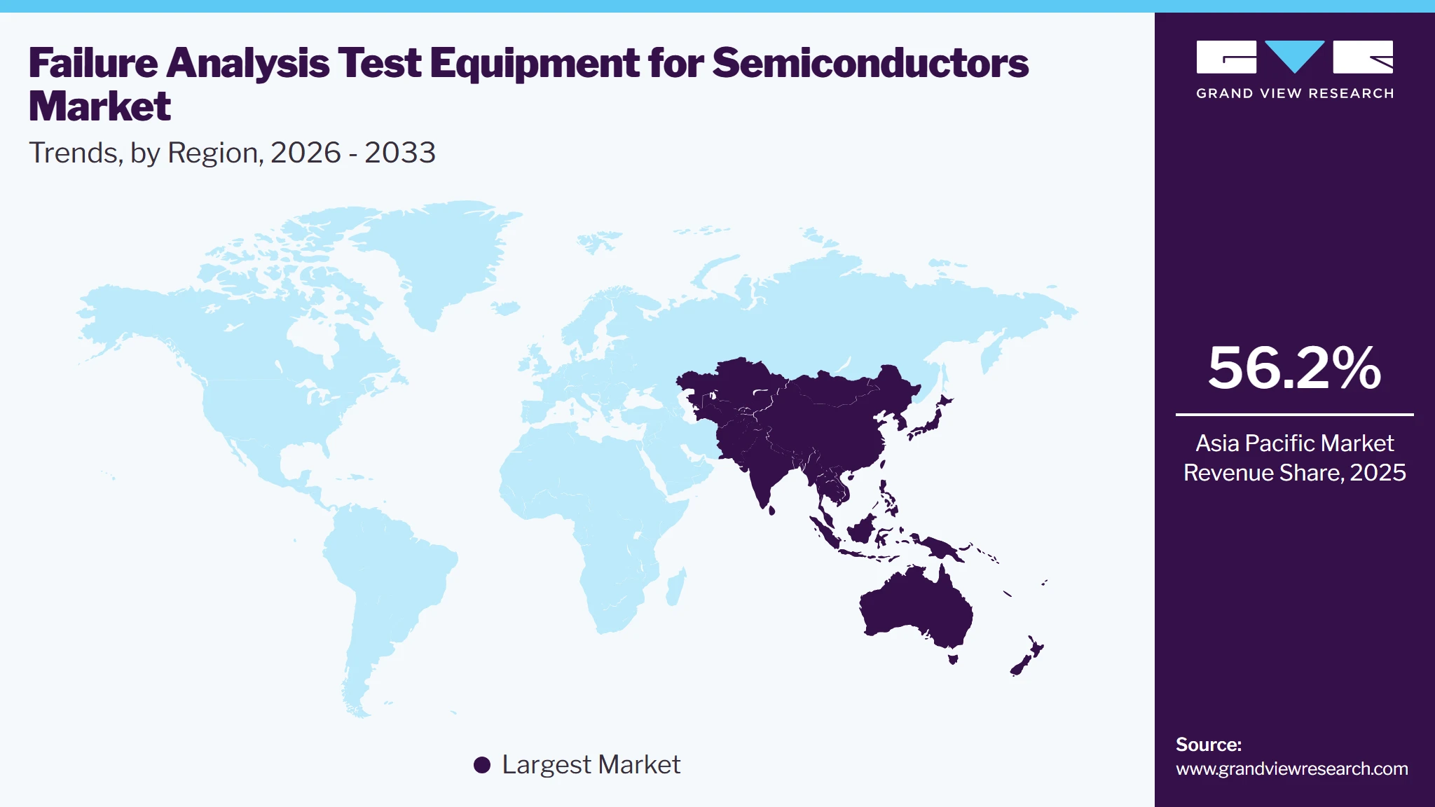
The global failure analysis test equipment for semiconductors market size was valued at USD 2.4 billion in 2025 and is projected to grow from USD 2.6 billion in 2026 to USD 4.5 billion by 2033, at a CAGR of 8.6% from 2026 to 2033. Asia Pacific dominated the failure analysis test equipment for semiconductors market with the largest revenue share of 56.2% in 2025. This growth of the failure analysis test equipment for semiconductors industry is driven by the increasing investments in semiconductor fabrication and rising R&D expenditures aimed at enhancing chip performance and reliability.
 Source: Grand View Research, IR Documents, Primary Interviews, Paid DatabasesTo learn more about this report,
 Download Free Sample Report
Key Market Trends & Insights
- By product: Scanning electron microscope (SEM) segment held the largest market share of 30.5% in 2025.
- By technology: Focused ion beam (FIB) segment held the largest market share of 19.9% in 2025.
Regional Highlights
- Largest regional market: Asia Pacific (56.2% revenue share, 2025)
- By country: China held the largest market share in 2025
Market Size & Forecast
- Market size in 2025: USD 2.4 Billion
- Estimated market size in 2026: USD 2.6 Billion
- Projected market size by 2033: USD 4.5 Billion
- CAGR (2026-2033): 8.6%
Prism AI by Grand View Research Free to tryAsk a question about the failure analysis test equipment for semiconductors marketTry asking✓Every figure cited from GVR research Prefer the report? Download free sample →Additionally, governments worldwide are implementing strategic initiatives to strengthen domestic semiconductor production, further fueling demand for advanced failure analysis test equipment.
 To learn more about this report, Download Free Sample Report
Market Dynamics
The failure analysis test equipment for semiconductors market is driven by the increasing complexity of semiconductor device architectures, continuous migration toward sub-5 nm process nodes, and the growing emphasis on yield enhancement, process optimization, and device reliability across advanced manufacturing environments. Rising investments in wafer fabrication facilities, heterogeneous integration, and advanced packaging technologies are further accelerating the deployment of high-resolution failure analysis solutions, including electron microscopy, focused ion beam (FIB), and nanoprobing systems. The proliferation of artificial intelligence, high-performance computing, automotive electronics, and 5G infrastructure is reinforcing the need for precise defect localization and root-cause analysis throughout the semiconductor value chain. However, market growth remains constrained by the substantial capital expenditure associated with advanced analytical instruments, lengthy procurement cycles, and the requirement for highly specialized technical expertise to operate sophisticated failure analysis platforms.
The increasing complexity of semiconductor manufacturing is a primary driver for the failure analysis test equipment for semiconductors market. As manufacturers transition to advanced process nodes, three-dimensional device architectures, and high-density integrated circuits, the need for precise defect characterization and root-cause analysis has intensified.
Growing production of semiconductors for artificial intelligence, automotive electronics, high-performance computing, and data center applications further reinforces demand for sophisticated failure analysis solutions that improve yield, accelerate process optimization, and ensure compliance with stringent reliability and quality standards.
High capital expenditure and significant technical complexity continue to restrain market growth. Advanced failure analysis platforms, including focused ion beam, electron microscopy, and nanoprobing systems, require substantial investment in equipment, laboratory infrastructure, and specialized operating environments.
Additionally, effective utilization depends on highly skilled personnel capable of conducting complex analytical workflows and interpreting nanoscale failure mechanisms, increasing both operational costs and implementation challenges for smaller market participants.
The accelerating adoption of advanced packaging technologies and heterogeneous integration presents a substantial growth opportunity for the failure analysis test equipment for semiconductors market. Innovations such as chiplet-based architectures, 2.5D/3D integration, through-silicon vias, and wafer-level packaging have significantly increased device complexity, creating greater demand for high-resolution analytical tools capable of evaluating package-level and interconnect failures.
As semiconductor manufacturers continue to prioritize performance, miniaturization, and reliability, investment in next-generation failure analysis equipment is expected to expand across both research and high-volume production environments.
Market Concentration & Characteristics
The global failure analysis test equipment for semiconductors industry is considerably fragmented characterized by a mix of large multinational companies and specialized regional players competing for market share. Key manufacturers focus on developing advanced failure analysis tools for semiconductor applications, aiming to enhance the performance and reliability of semiconductors. As the demand for high-quality and high-performance semiconductors rises, especially in industries such as consumer electronics, automotive, telecommunications, and healthcare, manufacturers are increasingly investing in sophisticated testing technologies to meet the needs for precise failure diagnostics and troubleshooting.
Innovation in the market is primarily driven by the need for enhanced efficiency, precision, and speed in failure analysis processes. With the increasing complexity of semiconductor devices, especially with the advent of 5G, AI, and Internet of Things (IoT) technologies, the demand for more advanced failure analysis test equipment, such as scanning electron microscopes (SEM), focused ion beam (FIB) systems, and X-ray inspection systems, is growing. Manufacturers are focusing on providing tools that can handle more intricate and smaller-scale components, as well as those that support rapid testing and data analysis.
 To learn more about this report, Download Free Sample Report
Regulatory standards and industry requirements play a significant role in shaping the failure analysis test equipment for semiconductors market, as semiconductor devices are subjected to stringent quality control and safety standards, particularly in industries such as automotive and healthcare. Compliance with these standards is crucial for manufacturers to maintain their competitiveness. Furthermore, the increasing focus on reducing product defects and enhancing yield in semiconductor manufacturing processes is driving the demand for failure analysis equipment capable of identifying even the minutest defects.
The market also faces competition from alternative testing methods and technologies, which may offer cost-effective solutions or quicker turnaround times. Manufacturers must continually innovate to integrate features like automation, artificial intelligence (AI), and real-time data analytics into their failure analysis systems to stay ahead in the market. Emphasizing reliability, precision, and the ability to analyze increasingly complex semiconductor devices will be key to capturing the growing demand for advanced failure analysis test equipment
Analyst Perspective
The failure analysis test equipment for semiconductors market is experiencing strong growth as semiconductor manufacturers increasingly invest in advanced inspection and diagnostic technologies to improve yield, accelerate product development, and ensure device reliability. The transition to smaller process nodes, heterogeneous integration, advanced packaging, and high-performance semiconductor devices has significantly increased the complexity of defect detection and root cause analysis. As a result, demand is rising for high-resolution analytical tools such as focused ion beam (FIB) systems, electron microscopes, X-ray inspection systems, and emission microscopy equipment. In addition, growing investments in artificial intelligence (AI), high-performance computing (HPC), automotive electronics, and advanced memory devices are driving continuous expansion of semiconductor manufacturing capacity.
Drivers, Opportunities & Restraints
Failure analysis test equipment is key in ensuring the integrity of semiconductor devices, as it allows manufacturers to detect minute imperfections that may compromise the functionality of these chips. As the complexity of semiconductor devices increases, with advanced packaging techniques and more intricate circuitry, the role of failure analysis test equipment becomes even more vital. The rising demand shows a growing emphasis on quality control and defect detection, which has led to greater investments in advanced testing equipment and techniques.
The high costs associated with failure analysis test equipment for semiconductor manufacturing significantly restrain the growth of the market. While the initial purchase price of these advanced instruments is a major consideration, companies often overlook several hidden costs that contribute to the total cost of ownership.
As the global automotive sector shifts towards EVs, there is a marked increase in the reliance on semiconductors for various critical functions, including battery management, powertrain control, charging systems, and vehicle connectivity. As a result, manufacturers are ramping up production of semiconductor devices tailored specifically for automotive applications in response to the growing demand for EVs.
Product Insights
Based on product, the scanning electron microscope (SEM) segment led the market with the largest revenue share of 30.5% in 2025. due to governments pushing the expansion of the semiconductor industry. SEM is crucial in semiconductor failure analysis for identifying surface defects, particle contamination, and structural anomalies at the nanoscale
The Focused Ion Beam (FIB) system is a versatile tool used in semiconductor failure analysis for imaging, milling, and modifying materials at the nanoscale. FIB systems direct a focused ion beam to etch, mill, or deposit material on a sample, allowing for precise manipulation and analysis of semiconductor structures. FIB is especially useful for sample preparation, defect analysis, and conducting cross-sectional imaging of complex semiconductor devices. The FIB segment is expected to experience robust growth due to its high versatility in failure analysis and its ability to work in tandem with other technologies such as SEM and TEM.
Technology Insights
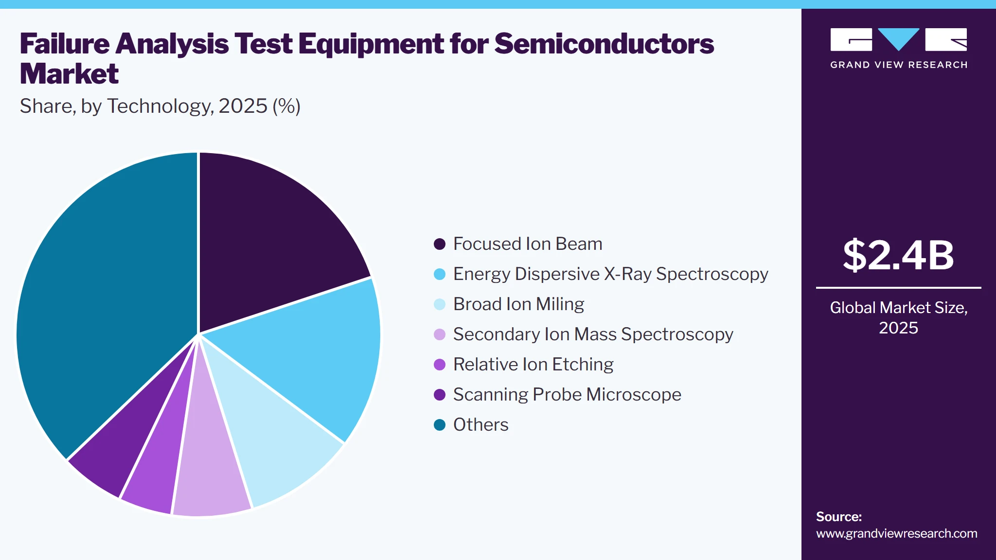
Based on technology, the focused ion beam (FIB) segment led the market with the largest revenue share of 19.9% in 2025, driven by its high versatility and ability to execute both imaging and sample preparation tasks. With the increasing complexity of semiconductor devices, FIB’s ability to inspect and repair structures at the nanoscale will be in high demand.
 To learn more about this report, Download Free Sample Report
The EDX segment is expected to maintain a significant share of the failure analysis test equipment for semiconductors market due to its high resolution and effectiveness in analyzing semiconductor materials. EDX’s ability to provide rapid and accurate elemental analysis is crucial as semiconductors become more complex, with smaller nodes and advanced materials. The segment is anticipated to grow steadily over the forecast period, driven by increasing demand for precision in analyzing defects in semiconductor components and expanding use in next-generation semiconductor devices.
Regional Insights
The growth of the failure analysis test equipment market in North America is primarily driven by advancements in semiconductor technology, increased investment in R&D, and the rising demand for high-performance electronics across industries like automotive, healthcare, and telecommunications. The presence of key semiconductor manufacturers and a strong focus on innovation in regions like Silicon Valley further support market expansion.
U.S. Failure Analysis Test Equipment For Semiconductors Market Trends
The industry in the U.S. is projected to expand at a CAGR of 8.6% over the forecast period,driven by the country's leadership in semiconductor innovation, with significant investments in R&D and manufacturing facilities. The presence of major semiconductor companies and the rapid advancement of technologies such as AI, 5G, and electric vehicles increase the demand for high-quality testing solutions.
Asia Pacific Failure Analysis Test Equipment For Semiconductors Market Trends
Asia Pacific dominated the failure analysis test equipment for semiconductors market with the largest revenue share of 56.2% in 2025. primarily due to the dominance of semiconductor manufacturing in countries like China, South Korea, Taiwan, and Japan. The growing electronics industry, especially in consumer electronics and mobile devices, coupled with significant investments in semiconductor production, accelerates the need for advanced testing solutions.
 To learn more about this report, Download Free Sample Report
The failure analysis test equipment for semiconductors market in China held the largest share in the Asia Pacific region in 2025. due to the country’s strong position as the world’s largest semiconductor producer. The government's heavy investment in semiconductor manufacturing and technology development, along with the rapid expansion of industries such as consumer electronics, automotive, and telecommunications, is fueling demand for advanced failure analysis.
The failure analysis test equipment for semiconductors market in India is expected to grow at a CAGR of 9.9% over the forecast period as the country becomes a key player in semiconductor design and manufacturing. The increasing demand for consumer electronics, mobile devices, and automotive technologies, coupled with government initiatives to boost semiconductor production under the "Make in India" program, is pushing the need for more efficient testing and failure analysis solutions. The growing focus on R&D in semiconductor technology also contributes to the market's expansion.
Europe Failure Analysis Test Equipment For Semiconductors Market Trends
In Europe, failure analysis test equipment for semiconductors industry growth is fueled by the increasing adoption of IoT devices, automotive electronics, and the rise of electric vehicles, all of which require high-quality semiconductor testing. The region's emphasis on sustainable and energy-efficient technologies also drives demand for failure analysis equipment, as manufacturers need to ensure product reliability and performance.
The failure analysis test equipment for semiconductors market in Germany is projected to expand at a CAGR of 7.1% over the forecast period as it benefits from the country's strong industrial base, particularly in automotive, industrial automation, and precision engineering. As Germany pushes forward with Industry 4.0 and the integration of more advanced electronics in manufacturing, there is an increasing need for high-quality semiconductors, driving demand for failure analysis testing..
The Spain failure analysis test equipment for semiconductors market is projected to expand at a CAGR of 6.3% over the forecast period as the country strengthens its position in the European semiconductor ecosystem. While Spain's semiconductor manufacturing base is smaller compared to other European countries, there is a rising demand for testing solutions driven by sectors such as automotive, telecommunications, and renewable energy.
Latin America Failure Analysis Test Equipment for Semiconductors Market Trends
In Latin America, the growth of the failure analysis test equipment industry is driven by the increasing penetration of electronics and the rising demand for quality control in semiconductor manufacturing. While the market is still developing, growing industrialization and the expansion of tech infrastructure are likely to boost demand for failure analysis solutions in the region.
The failure analysis test equipment for semiconductors market in Brazil is projected to expand at a CAGR of 6.6% over the forecast period as the country’s electronics and telecommunications sectors expand. While Brazil’s semiconductor manufacturing capabilities are still emerging, the increasing demand for consumer electronics, automotive applications, and industrial equipment is driving the need for high-quality failure analysis tools.
Middle East & Africa Failure Analysis Test Equipment for Semiconductors Market Trends
In the Middle East and Africa, the semiconductor market is expanding, supported by rising technological infrastructure investments and growing sectors like automotive and telecommunications. Though the market is in the early stages of development, increased government support for tech innovation and partnerships with global semiconductor players are likely to drive the adoption of failure analysis test equipment.
The Saudi Arabia failure analysis test equipment for semiconductors marketis projected to expand at a CAGR of 6.9% over the forecast period due to the country's diversification efforts under its Vision 2030 plan, which includes a focus on high-tech industries like electronics, automotive, and renewable energy. As Saudi Arabia looks to develop its semiconductor capabilities and reduce dependence on imports, the demand for failure analysis equipment is rising to ensure the quality and reliability of locally produced semiconductors.
Key Failure Analysis Test Equipment for Semiconductors Company Insights
Some of the key players operating in the market include HORIBA, Ltdand Emerson Electric Co.
-
Hitachi High-Technologies Corporation is a global company in high-tech solutions, offering advanced products and services across various sectors, including semiconductor manufacturing, healthcare, industrial equipment, and analytical instruments.
-
Thermo Fisher Scientific Inc. is the global leader in serving science, providing innovative solutions to customers across various sectors, including pharmaceutical and biotech companies, hospitals and clinical diagnostic labs, universities, research institutions, government agencies, and industries involved in environmental, industrial, research and development, and quality control.
Key Failure Analysis Test Equipment For Semiconductors Companies
The following key companies have been profiled for this study on the failure analysis test equipment for semiconductors market.
-
Thermo Fisher Scientific Inc.
-
Hitachi High-Technologies Corporation
-
Carl Zeiss AG
-
Oxford Instruments
-
HORIBA, Ltd.
-
Bruker
-
Jeol Ltd.
-
Tescan Orsay Holding
-
Imina Technologies SA.
-
Leica Microsystems
-
TED PELLA Inc
Competitive Benchmarking
Category
Operating Strategies
Competitive Edge
Weakness
Established Players (e.g., Thermo Fisher Scientific Inc., Hitachi High-Tech Corporation, Carl Zeiss AG, JEOL Ltd., KLA Corporation)
- Focus on continuous investment in high-resolution failure analysis technologies, integrating advanced imaging, sample preparation, and analytical capabilities into comprehensive platforms.
- Strengthen long-term partnerships with leading semiconductor manufacturers, foundries, and research institutes through customized solutions and lifecycle support services.
- Expand global manufacturing, application laboratories, and service networks to support advanced semiconductor process nodes and packaging technologies.
- Extensive product portfolios spanning electron microscopy, focused ion beam systems, spectroscopy, and integrated analytical solutions.
- Strong technological leadership supported by significant R&D investments, proprietary innovations, and established intellectual property portfolios.
- Broad global presence with strong customer relationships among leading semiconductor manufacturers and advanced research organizations.
- Premium pricing and high capital requirements can limit adoption among smaller semiconductor manufacturers and research facilities.
- Longer product development and commercialization cycles due to highly sophisticated technology platforms.
- Greater dependence on semiconductor capital expenditure cycles, resulting in demand fluctuations during industry downturns.
Emerging & Regional Players (e.g., Oxford Instruments plc, HORIBA, Ltd., Bruker Corporation, TESCAN ORSAY HOLDING a.s., Delmic B.V.)
- Premium pricing and high capital requirements can limit adoption among smaller semiconductor manufacturers and research facilities.
- Longer product development and commercialization cycles due to highly sophisticated technology platforms.
- Greater dependence on semiconductor capital expenditure cycles, resulting in demand fluctuations during industry downturns.
- Strong expertise in niche analytical technologies, enabling highly specialized solutions for advanced semiconductor failure analysis.
- Greater flexibility in product customization and faster response to evolving customer requirements.
- Competitive pricing and focused application support facilitate penetration into research laboratories and mid-sized semiconductor manufacturers.
- Limited product breadth compared with diversified global equipment manufacturers.
- Smaller international sales, distribution, and after-sales service networks may constrain large-scale market expansion.
- Lower financial resources and R&D budgets may limit the pace of technology development and commercialization compared with established industry leaders.
Recent Developments
-
In October 2024, TESCAN GROUP unveiled three advanced systems: SOLARIS X 2, SOLARIS 2, and AMBER X 2. These innovative systems are specifically developed to address the increasing demands of semiconductor failure analysis, offering enhanced precision, automation, and efficiency for technology nodes at sub-10 nm and beyond.
-
In August 2024, Oxford Instruments plc, a leading provider of high-tech products and services for industry and scientific research, completed the acquisition of FemtoTools AG, Switzerland. The company will now be part of Oxford Instruments' Imaging & Analysis division, where its products will complement the Group’s existing range of materials analysis tools, including electron microscope micro-analyzers and Raman microscopes
Failure Analysis Test Equipment for Semiconductors Market Report Scope
Report Attribute
Details
Market size in 2025
USD 2.4 billion
Estimated market size in 2026
USD 2.6 billion
Projected market size by 2033
USD 4.5 billion
Growth rate
CAGR of 8.6% from 2026 to 2033
Base year for estimation
2025
Historical data
2021 – 2024
Forecast period
2026 - 2033
Quantitative units
Revenue in USD billion and CAGR from 2026 to 2033
Report coverage
Revenue forecast, company ranking, competitive landscape, growth factors, and trends
Segments covered
Product, technology, region
Regional scope
North America; Europe; Asia Pacific; Latin America; Middle East & Africa
Country scope
U.S.; Canada; Mexico; UK; Germany; France; Italy; Spain; China; India; Japan; South Korea; Australia; Taiwan; Brazil; Argentina; Israel; Saudi Arabia; UAE
Key companies profiled
Thermo Fisher Scientific Inc., Hitachi High-Tech Corporation, Carl Zeiss AG, Oxford Instruments plc, HORIBA, Ltd., JEOL Ltd., Bruker Corporation, TESCAN ORSAY HOLDING a.s., KLA Corporation, and Delmic B.V.
Customization scope
Free report customization (equivalent up to 8 analysts' working days) with purchase. Addition or alteration to country, regional & segment scope.
Pricing and purchase options
Avail customized purchase options to meet your exact research needs. Explore purchase options
Global Failure Analysis Test Equipment For Semiconductors Market Report Segmentation
This report forecasts revenue growth at global, regional & country levels and provides an analysis on the industry trends in each of the sub-segments from 2021 to 2033. For this study, Grand View Research has segmented the global failure analysis test equipment for semiconductors market based on product, technology, and region:
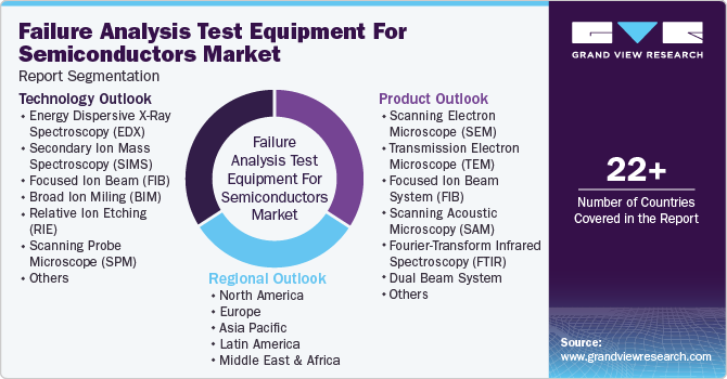 To learn more about this report, Download Free Sample Report
-
Product Outlook (Revenue, USD Million, 2021 - 2033)
-
Scanning Electron Microscope (SEM)
-
Transmission Electron Microscope (TEM)
-
Focused Ion Beam System (FIB)
-
Scanning Acoustic Microscopy (SAM)
-
Fourier-Transform Infrared Spectroscopy (FTIR)
-
Dual Beam System
-
Others
-
-
Technology Outlook (Revenue, USD Million, 2021 - 2033)
-
Energy Dispersive X-Ray Spectroscopy (EDX)
-
Secondary Ion Mass Spectroscopy (SIMS)
-
Focused Ion Beam (FIB)
-
Broad Ion Miling (BIM)
-
Relative Ion Etching (RIE)
-
Scanning Probe Microscope (SPM)
-
Others
-
-
Regional Outlook (Revenue, USD Million, 2021 - 2033)
-
North America
-
U.S.
-
Canada
-
Mexico
-
-
Europe
-
UK
-
France
-
Germany
-
Italy
-
Spain
-
-
Asia Pacific
-
China
-
India
-
Japan
-
South Korea
-
Taiwan
-
Australia
-
-
Latin America
-
Brazil
-
Argentina
-
-
Middle East & Africa
-
Israel
-
Saudi Arabia
-
UAE
-
-
Research Methodology
The failure analysis test equipment for semiconductors market figures in this report are based on a proven research process that combines executive interviews with secondary research from proprietary databases, company filings, and recognized regulatory and institutional sources. Market size is built through value-chain sizing - reconciling supply-side and demand-side estimates - and triangulated with bottom-up and top-down approaches. Every estimate passes multiple levels of expert validation before publication, with each failure analysis test equipment for semiconductors segment quantified using the revenue-capture definitions in the table below.
Segment Definition
Segment - Product
Revenue Capture Definition
Scanning Electron Microscope (SEM)
Revenue generated from the sale of standalone and integrated scanning electron microscope (SEM) systems, including semiconductor-specific configurations designed for failure analysis and materials characterization.
Transmission Electron Microscope (TEM)
Revenue generated from the sale of transmission electron microscope (TEM) systems, including high-resolution analytical platforms and semiconductor-focused configurations for advanced failure analysis.
Focused Ion Beam System (FIB)
Revenue generated from the sale of focused ion beam (FIB) systems, including gallium and plasma FIB platforms configured for semiconductor failure analysis and precision sample preparation.
Scanning Acoustic Microscopy (SAM)
Revenue generated from the sale of scanning acoustic microscopy (SAM) systems, including laboratory-grade and industrial inspection platforms for semiconductor package analysis.
Fourier-Transform Infrared Spectroscopy (FTIR)
Revenue generated from the sale of Fourier-transform infrared spectroscopy (FTIR) systems, including benchtop and integrated analytical instruments utilized in semiconductor material characterization.
Dual Beam System
Revenue generated from the sale of integrated dual beam (FIB-SEM) platforms combining electron and ion beam technologies for advanced semiconductor failure analysis.
Others
Revenue generated from the sale of other semiconductor failure analysis equipment, including X-ray microscopy systems, nanoprobing platforms, optical inspection systems, laser-based analytical instruments, and related specialized equipment.
Segment – Technology
Revenue Capture Definition
Energy Dispersive X-Ray Spectroscopy (EDX)
Revenue generated from the sale of energy dispersive X-ray spectroscopy (EDX) systems, detectors, and integrated elemental analysis solutions for semiconductor failure analysis.
Secondary Ion Mass Spectroscopy (SIMS)
Revenue generated from the sale of secondary ion mass spectrometry (SIMS) systems, including dynamic and static SIMS platforms for semiconductor analytical applications.
Focused Ion Beam (FIB)
Revenue generated from the sale of failure analysis platforms incorporating focused ion beam (FIB) technology, including standalone and integrated analytical systems.
Broad Ion Milling (BIM)
Revenue generated from the sale of broad ion milling (BIM) systems and associated sample preparation platforms designed for semiconductor analytical workflows.
Reactive Ion Etching (RIE)
Revenue generated from the sale of reactive ion etching (RIE) systems utilized for semiconductor deprocessing, layer removal, and analytical sample preparation.
Scanning Probe Microscope (SPM)
Revenue generated from the sale of scanning probe microscope (SPM) systems, including atomic force microscopy (AFM) and related nanoscale characterization platforms for semiconductor analysis.
Others
Revenue generated from the sale of other failure analysis technologies, analytical platforms, and specialized characterization systems not included within the above technology categories.
Estimation Model
Layer No.
Layer Name
Key Question
Description
01
Semiconductor Manufacturing Base Layer
Which facilities represent the addressable market?
Quantify semiconductor fabrication facilities across integrated device manufacturers (IDMs), foundries, outsourced semiconductor assembly and test (OSAT) providers, advanced packaging facilities, and research laboratories. Model wafer production capacity, technology node distribution, and regional manufacturing intensity to determine the addressable installed base.
02
Failure Analysis Demand Layer
Which facilities require failure analysis test equipment?
Assess the proportion of semiconductor facilities requiring failure analysis equipment based on technology node advancement, product reliability requirements, yield improvement initiatives, advanced packaging complexity, and research & development activities.
03
Technology Adoption Layer
What share of facilities utilize advanced failure analysis technologies?
Estimate penetration of SEM, TEM, FIB, Dual Beam, SAM, FTIR, EDX, SIMS, BIM, RIE, and SPM technologies by semiconductor application, manufacturing stage, end user, and geography while accounting for equipment replacement cycles and laboratory sophistication.
04
Revenue Generation Layer
How is market revenue generated?
Estimate annual shipments of failure analysis test equipment by equipment type, application, end-use industry, and region. Quantify revenues generated exclusively from the sale of new failure analysis test equipment supplied to semiconductor manufacturers, foundries, OSAT companies, research laboratories, and academic institutions.
Delivered Customizations
This report has been delivered with the following In-depth customizations
Client Request
Customization Delivered
Value Adds
Competitive Benchmarking
Benchmarked leading failure analysis test equipment for semiconductors manufacturers based on product portfolio strength, technology capabilities, financial strength, geographic presence, end-user focus, and strategic positioning, while differentiating established market leaders from emerging technology providers.
Provided a comprehensive view of the competitive landscape, enabling the client to evaluate competitive positioning, identify technology differentiation, benchmark innovation capabilities, and assess strategic growth opportunities.
Regional Segmentation
Refined regional analysis by evaluating semiconductor manufacturing capacity, wafer fabrication investments, advanced packaging adoption, R&D intensity, government semiconductor initiatives, and technology node migration across North America, Europe, Asia Pacific, Latin America, and the Middle East & Africa.
Enabled identification of high-growth regional markets, manufacturing investment hubs, and technology adoption trends, supporting regional expansion strategies and resource allocation decisions.
Opportunity Assessment
Assessed emerging growth opportunities across advanced process nodes, heterogeneous integration, chiplet architectures, AI and high-performance computing semiconductors, advanced packaging technologies, and next-generation failure analysis platforms incorporating automation and high-resolution analytical capabilities.
Helped prioritize high-value investment opportunities by identifying rapidly expanding semiconductor applications, evolving technology requirements, and the most attractive future revenue segments across the semiconductor value chain.
Frequently Asked Questions About This Report
Asia Pacific is anticipated to be one of the fastest-growing regional markets over the forecast period, driven by expanding semiconductor fabrication capacity, increasing government support for domestic chip manufacturing, and rising investments in advanced packaging and process technologies.
The scanning electron microscope (SEM) segment led the market with the largest revenue share of 30.5% in 2025.
The focused ion beam (FIB) segment accounted for the largest revenue share of 19.9% in 2025.
Key trends include increasing adoption of high-resolution electron microscopy and focused ion beam technologies, integration of AI-assisted defect analysis, growing demand for advanced failure analysis tools for sub-5 nm semiconductor nodes, and rising investments in advanced packaging and chip reliability testing.
The global failure analysis test equipment for semiconductors market size was estimated at USD 2.4 billion in 2025 and is expected to be USD 2.6 billion in 2026.
The global failure analysis test equipment for semiconductors market, in terms of revenue, is expected to grow at a compound annual growth rate of 8.6% from 2026 to 2033 to reach USD 4.5 billion by 2033.
Asia Pacific dominated the failure analysis test equipment for semiconductors market with the largest revenue share of 56.2% in 2025.
Some of the key players operating in the Failure Analysis Test Equipment for Semiconductors Market are Thermo Fisher Scientific Inc., Hitachi High-Technologies Corporation, Carl Zeiss AG, Oxford Instruments, HORIBA, Ltd., Bruker, Jeol Ltd., Tescan Orsay Holding, Imina Technologies SA., Leica Microsystems, TED PELLA Inc.
Key factors driving the failure analysis test equipment market for semiconductors include the increasing demand for advanced electronics, high-performance semiconductors, and technological advancements in R&D. Additionally, the push for improved product reliability and quality control across industries like automotive, telecommunications, and consumer electronics is fueling growth.
About the Author(s)
Advanced Interior Materials Research Team
Advanced Materials · Advanced Interior MaterialsThis report was authored by the advanced interior materials research team at Grand View Research - comprising two research analysts, one senior research analyst, and one industry expert - with specialized expertise in the advanced interior materials segment of the advanced materials industry. All findings are based on proprietary advanced materials databases, executive interviews, and regulatory analysis, subject to internal peer review prior to publication.
Last Updated:
Speak to Analyst

Customize this report to your needs - add regions, segments, or data points, with 20% free customization.
Or view our licence options:


ISO 9001:2015 & 27001:2022 Certified
We are GDPR and CCPA compliant! Your transaction & personal information is safe and secure. For more details, please read our privacy policy.


