- Home
- »
- Advanced Interior Materials
- »
-
Wafer Vacuum Assembling Equipment Market Report, 2026-2033GVR Report cover
![Wafer Vacuum Assembling Equipment Market (2026 - 2033)Report]()
Wafer Vacuum Assembling Equipment Market (2026 - 2033)
Size, Share & Trends Analysis Report By Product (Fully Automatic Vacuum Assembling Equipment), By Application (Semiconductor Industry, Solar Panel Manufacturing), By Region, And Segment Forecasts
Market Size, 2023
$2.3BMarket Estimate, 2026
$2.5BMarket Forecast, 2033
$3.6BCAGR, 2024–2033
5.5%Wafer Vacuum Assembling Equipment Market Summary
The global wafer vacuum assembling equipment market size was valued at USD 2.3 billion in 2025 and is projected to grow from USD 2.5 billion in 2026 to USD 3.6 billion by 2033, at a CAGR of 5.5% from 2026 to 2033. Asia Pacific dominated the market, accounting for a revenue share of 69.4% in 2025. The demand for wafer vacuum assembling equipment is on a significant upswing, fueled by the growth in the semiconductor industry.

Key Market Trends & Insights
- By product: Semi-automatic vacuum assembling equipment segment led the market with the largest revenue share of 41.6% in 2025.
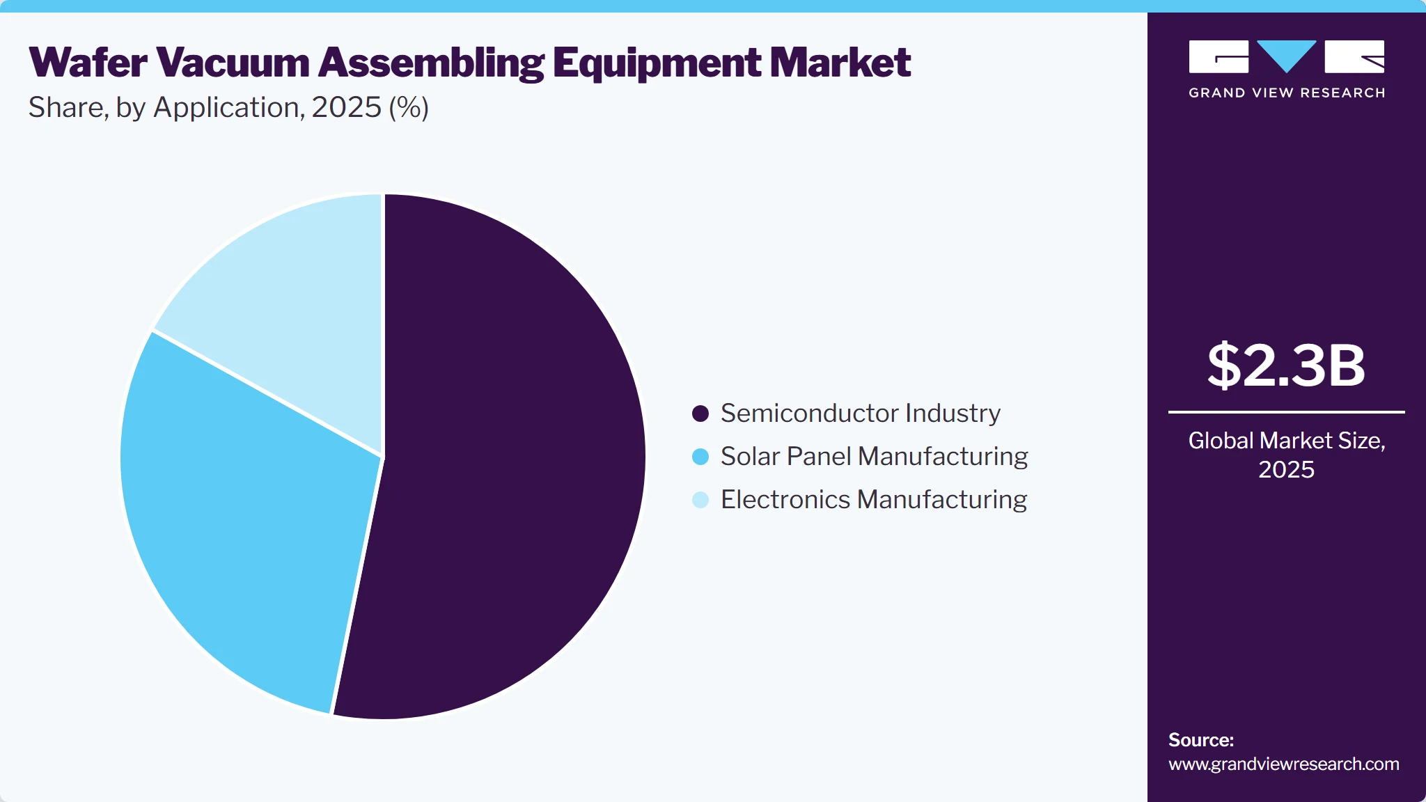
- By application: Semiconductor industry segment led the market with the largest revenue share of 53.2% in 2025
Regional Highlights
- Largest regional market: Asia Pacific (69.4% revenue share, 2025)
- By country: The China held the largest market share in 2025.
Market Size & Forecast
- Market size in 2025: USD 2.3 Billion
- Estimated market size in 2026: USD 2.5 Billion
- Projected market size by 2033: USD 3.6 Billion
- CAGR (2026-2033): 5.5%
The rising demand for wafer vacuum assembling equipment is driven by the miniaturization of electronic devices, compelling chip manufacturers to pursue advancements in wafer-level packaging, where vacuum assembling plays a crucial role in ensuring the integrity and performance of ultra-thin wafers. Moreover, the rise of 5G technology and the onset of the 6G horizon are pushing the boundaries for faster, more efficient semiconductor components.

This telecommunication evolution necessitates the fabrication of sophisticated chips, where vacuum assembly processes are indispensable for achieving the high precision and reliability required. Additionally, the automotive sector's swift move toward electric vehicles (EVs) and autonomous driving technology creates a new demand avenue. The semiconductors needed for these innovations must be of the highest quality, driving the need for advanced vacuum assembling equipment to produce power electronics, sensors, and control units.
Market Dynamics
The wafer vacuum assembling equipment market is shaped by continuous advancements in semiconductor fabrication, growing adoption of advanced packaging technologies, increasing chip complexity, and expanding investments in wafer-level manufacturing facilities. The transition toward 3D integration, heterogeneous packaging, MEMS, power semiconductors, and compound semiconductor devices is driving demand for highly precise vacuum assembly systems that ensure superior bonding accuracy, contamination control, and process stability. At the same time, stringent yield requirements, cleanroom manufacturing standards, high equipment costs, process integration challenges, and fluctuations in semiconductor capital expenditure influence technology adoption, production planning, and competitive positioning across the global market.
The growing use of wafer-level packaging (WLP), 2.5D/3D integration, and hybrid bonding is accelerating demand for high-precision wafer vacuum assembling equipment. Semiconductor manufacturers are prioritizing equipment capable of delivering accurate alignment, void-free bonding, and controlled vacuum environments to achieve higher device performance and production yields. Continuous investment in advanced logic, memory, and power semiconductor manufacturing further strengthens equipment deployment across fabrication and packaging facilities.
Wafer vacuum assembling equipment requires substantial capital investment, advanced cleanroom infrastructure, and highly specialized process expertise. Integrating these systems into existing semiconductor production lines often involves extensive qualification, calibration, and compatibility assessments. Long equipment procurement cycles and high maintenance requirements can also limit adoption, particularly among smaller semiconductor manufacturers and outsourced assembly providers.
The increasing commercialization of compound semiconductors, silicon photonics, and heterogeneous integration presents significant growth opportunities for wafer vacuum assembling equipment manufacturers. These applications require advanced bonding processes with stringent precision and contamination control. Growing investments in AI processors, high-performance computing, automotive electronics, and next-generation communication devices are creating sustained demand for innovative vacuum assembly solutions with higher throughput and process flexibility.
Analyst Perspective
The wafer vacuum assembling equipment market is expanding as semiconductor manufacturers invest in advanced packaging technologies requiring high-precision wafer bonding under controlled vacuum conditions. Increasing semiconductor complexity and the adoption of 3D packaging, heterogeneous integration, MEMS, power semiconductors, and optoelectronic devices are driving demand for high-precision equipment. Investments in semiconductor fabrication and advanced packaging across Asia Pacific, North America, and Europe are boosting demand for automated vacuum assembly systems. Advancements in automation, precision motion control, and intelligent process monitoring are improving manufacturing efficiency. As manufacturers develop next-generation chip architectures and improve production yields, suppliers of automated, application-specific wafer vacuum assembling equipment are expected to benefit from sustained long-term market growth.
Drivers, Opportunities & Restraints
The primary drivers of the market include the relentless technological advancement and the exponential growth of the consumer electronics sector. The incessant demand for smaller, more powerful, and energy-efficient devices necessitates sophisticated semiconductor chips, which require precise wafer vacuum assembling processes. Moreover, emerging technologies such as 5G, AI, IoT, and autonomous vehicles are pushing the boundaries of semiconductor capabilities, demanding higher precision and reliability from wafer assembly processes. Additionally, the global push toward electrification and sustainable technologies is fueling the need for more advanced semiconductors, directly impacting the demand for high-precision wafer vacuum assembling equipment.
One significant opportunity within the sector lies in the expansion of semiconductor manufacturing capabilities globally, spurred by the need to secure and diversify supply chains, especially in the wake of recent global disruptions. This global expansion represents a fertile ground for the deployment of new wafer vacuum assembling solutions. Furthermore, the shift toward more advanced packaging technologies, such as 3D packaging, and the increasing adoption of silicon carbide (SiC) and gallium nitride (GaN) in power electronics present substantial opportunities for innovation and growth within the equipment market. The push for more sustainable and energy-efficient manufacturing processes also opens avenues for advancements in vacuum technology, offering opportunities for equipment manufacturers to lead in green manufacturing initiatives.
However, the market faces several restraints, including the high costs associated with adopting and maintaining cutting-edge wafer vacuum assembling equipment. The significant investment required for advanced machinery can be a barrier for smaller manufacturers, potentially limiting market growth. Additionally, the complex technical requirements and the need for highly specialized skills for operating such equipment pose challenges for workforce development and can affect the rate of adoption. Finally, the rapid pace of technological change, while a driver of demand, also presents a restraint as equipment can quickly become obsolete, requiring continuous research and development efforts and investments to stay competitive and meet the evolving needs of the semiconductor industry.
Product Insights
Based on product, the semi-automatic vacuum assembling equipment segment led the market with the largest revenue share of 41.6% in 2025. The shift toward digitalization and smart manufacturing practices has propelled the demand for fully automatic vacuum assembling equipment to unprecedented levels. This surge is primarily driven by the semiconductor industry's pursuit of higher throughput, superior precision, and enhanced productivity to meet the escalating demands for advanced consumer electronics, automotive components, and IoT devices. Fully automatic systems offer significant advantages in terms of reduced human error, consistent product quality, and the ability to operate continuously, which significantly improves production efficiency and cost-effectiveness.
The demand for manual vacuum assembling equipment remains steady, particularly in niche markets and among small to medium-sized enterprises that derive value from the flexibility and lower initial costs of these systems. These manual systems are favored for certain specialized applications where the precision and customization offered by hands-on operation are paramount or where the scale of production does not justify the hefty investment in fully automatic systems. Moreover, in research and development environments, where the assembly requirements can frequently change, manual vacuum assembling equipment offers the adaptability needed without significant reconfiguration costs. Despite the trend toward automation, the demand for manual equipment is sustained by its affordability, ease of modification, and suitability for low-volume, high-precision tasks.
Application Insights
Based on application, the semiconductor industry segment led the market with the largest revenue share of 53.2% in 2025. In the semiconductor industry, wafer vacuum assembly equipment plays a crucial role in the fabrication and assembly of semiconductor devices. These sophisticated machines are used for processes such as wafer bonding, chip encapsulation, and the precise alignment of wafer layers under vacuum conditions to ensure flawless adhesion without contaminants or air bubbles. The vacuum environment is essential for achieving the high level of precision and cleanliness required in semiconductor manufacturing, where even the smallest impurity or misalignment can lead to the failure of the semiconductor device. The increasing complexity of semiconductor devices, with more layers and finer circuits, has made the role of vacuum assembly equipment more critical than ever. This technology enables the mass production of semiconductors with high yield rates and reliability, supporting the rapid advancement and miniaturization of electronic devices.
In electronics manufacturing, wafer vacuum assembly equipment is utilized in the production of various components, such as sensors, MEMS (Micro-Electro-Mechanical Systems), and LEDs, which are integral to modern electronic devices. The use of vacuum assembly ensures that these components are manufactured within strictly controlled environments, minimizing the risk of contamination that could impair their performance or longevity. Particularly in the production of MEMS, which often combines mechanical and electrical components in a single silicon chip, the precision and environmental control provided by vacuum assembly are indispensable. This technology facilitates the integration of these components into a wide array of consumer electronics, automotive technologies, and medical devices, among others, enabling the development of smaller, more efficient, and reliable products. The push for greater functionality and compactness in electronic devices continues to drive the demand for wafer vacuum assembly equipment within the electronics manufacturing sector.
Regional Insights
North America wafer vacuum assembling equipment market is growing as in this region, particularly in the U.S., the semiconductor industry is a pivotal sector, with the demand for wafer vacuum assembling equipment being robust and consistently driven by the innovation-centric technology landscape. The U.S. government's focus on revitalizing domestic semiconductor manufacturing capacity, exemplified by significant investments and policy support, underscores the strategic importance of this sector. This environment fosters a strong demand for cutting-edge semiconductor production technologies, including advanced vacuum assembling systems, to maintain competitiveness and security in the global technology arena. Furthermore, the presence of leading semiconductor companies and research institutions contributes to sustained demand for sophisticated wafer vacuum assembling machinery to facilitate the development of next-generation semiconductor technologies.
Asia Pacific Wafer Vacuum Assembling Equipment Market Trends
Asia Pacific dominated the wafer vacuum assembling equipment market with the largest revenue share of 69.4%in 2025, driven by the rapid expansion of the semiconductor industry in countries such as China, South Korea, Taiwan, and Japan. This region is home to some of the world's largest semiconductor foundries and electronics manufacturers, necessitating state-of-the-art production capabilities to meet both domestic and global electronics demand. The continuous push for technological advancements, coupled with substantial investments in semiconductor manufacturing expansion and upgrades, fuels the demand for sophisticated wafer vacuum assembling systems. Furthermore, the region's role as a global electronics manufacturing hub, exporting to international markets, ensures sustained high demand for such equipment to maintain efficiency and production quality standards.

India wafer vacuum assembling equipment market is witnessing a notable increase, primarily driven by the country's burgeoning electronics manufacturing sector and ambitious government initiatives aimed at boosting the domestic production of semiconductors. With policies like the 'Make in India' campaign, there is a significant push toward establishing India as a hub for semiconductor manufacturing, attracting investments from both national and international entities. Additionally, the country's expansive consumer electronics market, one of the largest globally, underscores a compelling need for localized semiconductor production capabilities, further propelling the demand for high-precision equipment like wafer vacuum assemblers. As India gradually makes strides toward self-reliance in semiconductor production, the demand for such specialized equipment is expected to grow steadily.
China Wafer Vacuum Assembling Equipment Market Trends
The wafer vacuum assembling equipment market in China held the largest share in the Asia Pacific region in 2025.
Europe Wafer Vacuum Assembling Equipment Market Trends
The wafer vacuum assembling equipment market in Europe is heavily influenced by its strong automotive industry, renewable energy initiatives, and a strategic focus on enhancing semiconductor manufacturing capabilities within the region. European semiconductor manufacturers are increasingly investing in advanced manufacturing technologies to produce high-quality, energy-efficient chips essential for electric vehicles (EVs), smart grids, and IoT applications. Additionally, the European Union's initiatives to bolster technological sovereignty and reduce dependency on external semiconductor supplies spark investments in local semiconductor production, further driving the demand for specialized equipment like wafer vacuum assemblers. Europe's approach to greener and more sustainable manufacturing processes also emphasizes the need for advanced, efficient assembly equipment in the semiconductor sector.
Key Wafer Vacuum Assembling Equipment Company Insights
Some of the key players operating in the market include Applied Materials Inc., Lam Research Corporation, KLA Corporation, among others.
-
Applied Materials Inc. operates in three business segments, namely Semiconductor systems, applied global services (AGS), display, and adjacent markets. The semiconductor systems market develops, manufactures, and sells a diverse range of manufacturing equipment used to fabricate the semiconductor chips, termed as ICs. The AGS segment provides solutions to optimize fab performance and productivity, including upgrades, spares, and services. It also provides solutions to optimize the earlier generation equipment and factory automation software for semiconductors, displays, and other products.
-
Lam Research Corporation is a USA-based wafer fabrication equipment manufacturer and related service provider in the semiconductor industry. It designs and builds products in front-end wafer processing, including equipment for thin film deposition, photoresist strips, and plasma etch. The company provides manufacturing and servicing of wafer-processing semiconductor manufacturing equipment. It allows customers to build smaller and better-performing devices.
Ted Pella, Inc. and AMAC Technologies are some of the emerging market participants in the wafer vacuum assembling equipment market.
-
Ted Pella, Inc. is a family-owned American company specializing in manufacturing and distributing high-quality tools and equipment for microscopy and related fields. Established in 1968 and headquartered in Redding, California, the company has built a reputable standing in the market for supplying a wide range of products, including microscopes, specimen preparation tools, and vacuum assembling equipment. Their product offerings cater to various sectors, such as research and development, materials science, electronics, and biomedical sciences. Ted Pella, Inc. is known for its commitment to quality, customer service, and innovation, constantly expanding its product line to meet the evolving needs of scientists and researchers worldwide.
-
AMAC Technologies stands at the forefront of vacuum sealing and packaging solutions, providing advanced and efficient machinery for various industries, including food, pharmaceutical, and electronics. Since its establishment, the company has been dedicated to innovation, designing equipment that enhances productivity, preserves product integrity, and extends shelf life. AMAC Technologies is recognized for its comprehensive range of products, from fully automatic vacuum packaging systems to specialized vacuum sealing equipment. The company prides itself on offering custom-tailored solutions that address specific customer needs and exceptional customer service. With a focus on technology-driven solutions and sustainability, AMAC Technologies continues to lead in providing vacuum packaging equipment that meets the rigorous demands of modern industry standards.
Key Wafer Vacuum Assembling Equipment Companies
The following key companies have been profiled for this study on the wafer vacuum assembling equipment market.
- Shin-Etsu Chemical Co., Ltd.
- Nitto Denko Corporation
- H-Square Corporation
- Ted Pella, Inc.
- AMAC Technologies
- SIPEL ELECTRONIC SA
- Hefei TREC Precision Equipment Co., Ltd.
- Applied Materials Inc.
- Tokyo Electron Limited
- Lam Research Corporation
- KLA Corporation
Competitive Benchmarking
Category
Operating Strategies
Competitive Edge
Weakness
Established Players (e.g., Applied Materials, Inc.; Tokyo Electron Limited (TEL); EV Group (EVG); SUSS MicroTec SE; BE Semiconductor Industries N.V. (Besi); ASMPT Limited; Shibaura Mechatronics Corporation)
- Invest in advanced wafer bonding, hybrid bonding, and vacuum assembly technologies while expanding automation and AI-enabled process control.
- Strengthen global service networks and collaborate with leading semiconductor foundries, IDMs, and OSATs to support next-generation packaging applications.
- Strong technological expertise, extensive patent portfolios, and established customer relationships enable high-precision, high-throughput equipment with proven manufacturing reliability.
- Broad global presence, comprehensive after-sales support, and integrated semiconductor equipment portfolios enhance long-term competitiveness.
- High equipment costs and lengthy product qualification cycles can slow customer adoption.
- Dependence on semiconductor capital expenditure makes revenues sensitive to industry investment cycles and demand fluctuations.
Emerging & Regional Players (e.g., Hefei TREC Precision Equipment Co., Ltd.; Canon Machinery Inc.; BONDTECH Co., Ltd.)
- Focus on cost-competitive wafer bonding and vacuum assembly solutions tailored to regional semiconductor manufacturers and niche advanced packaging applications.
- Expand domestic manufacturing capabilities and strengthen partnerships with research institutes and local semiconductor fabs to improve market penetration.
- Competitive pricing, application-specific customization, and faster response to regional customer requirements support growth in emerging semiconductor manufacturing hubs.
- Flexibility in product development allows rapid adaptation to evolving packaging technologies and customer specifications.
- Limited global brand recognition and smaller international sales networks compared with established competitors.
- Lower R&D budgets and narrower product portfolios may restrict participation in the most advanced semiconductor manufacturing projects.
Recent Developments
-
In October 2023, SA-Foundry sp. z o.o. finalized the creation of a state-of-the-art facility designed to produce premium aluminum alloy castings through the High Pressure Die Casting (HPDC) method for a new client. This newly established HPDC facility is customized to meet the specific needs of the client, enabling them to enhance their output of superior aluminum alloy castings.
Wafer Vacuum Assembling Equipment Market Report Scope
Report Attribute
Details
Market size in 2025
USD 2.3 billion
Estimated market size in 2026
USD 2.5 billion
Projected market size by 2033
USD 3.6 billion
Growth rate
CAGR of 5.5% from 2026 to 2033
Base year for estimation
2025
Historical data
2021 - 2024
Forecast period
2026 - 2033
Quantitative units
Revenue in USD billion and CAGR from 2026 to 2033
Report coverage
Revenue forecast, company ranking, competitive landscape, growth factors, and trends
Segments covered
Product, application, and region
Regional scope
North America; Europe; Asia Pacific; Latin America; Middle East & Africa
Country scope
U.S., Canada, Mexico, Germany, France, Italy, UK, Spain, China, Japan, India, South Korea, Australia, Brazil, Argentina, South Africa, Saudi Arabia, UAE
Key companies profiled
Applied Materials, Inc.; Tokyo Electron Limited (TEL); EV Group (EVG); SUSS MicroTec SE; BE Semiconductor Industries N.V. (Besi); ASMPT Limited; Shibaura Mechatronics Corporation; Hefei TREC Precision Equipment Co., Ltd.; Canon Machinery Inc.; BONDTECH Co., Ltd.
Customization scope
Free report customization (equivalent up to 8 analysts' working days) with purchase. Addition or alteration to country, regional & segment scope.
Pricing and purchase options
Avail customized purchase options to meet your exact research needs. Explore purchase options
Global Wafer Vacuum Assembling Equipment Market Report Segmentation
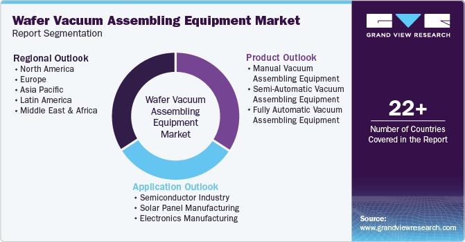
This report forecasts revenue growth at global, regional & country levels and provides an analysis of the latest industry trends in each of the sub-segments from 2021 to 2033. For this study, Grand View Research has segmented the global wafer vacuum assembling equipment market report on the basis of product, application, and region:
-
Product Outlook (Revenue, USD Million, 2021 - 2033)
-
Manual Vacuum Assembling Equipment
-
Semi-Automatic Vacuum Assembling Equipment
-
Fully Automatic Vacuum Assembling Equipment
-
-
Application Outlook (Revenue, USD Million, 2021 - 2033)
-
Semiconductor Industry
-
Solar Panel Manufacturing
-
Electronics Manufacturing
-
-
Regional Outlook (Revenue, USD Million, 2021 - 2033)
-
North America
-
U.S.
-
Canada
-
Mexico
-
-
Europe
-
UK
-
Germany
-
France
-
Italy
-
Spain
-
-
Asia Pacific
-
Japan
-
China
-
India
-
Australia
-
South Korea
-
-
Latin America
-
Brazil
-
Argentina
-
-
Middle East & Africa
-
South Africa
-
Saudi Arabia
-
UAE
-
-
Research Methodology
The wafer vacuum assembling equipment market figures in this report are based on a proven research process that combines executive interviews with secondary research from proprietary databases, company filings, and recognized regulatory and institutional sources. Market size is built through value-chain sizing - reconciling supply-side and demand-side estimates - and triangulated with bottom-up and top-down approaches. Every estimate passes multiple levels of expert validation before publication, with each wafer vacuum assembling equipment segment quantified using the revenue-capture definitions in the table below.
Segment Definition
Segment - Product
Revenue Capture Definition
Manual Vacuum Assembling Equipment
Revenue is generated from the sale of manually operated wafer vacuum assembling equipment designed for research, prototype development, and low-volume production, offering precision wafer alignment and vacuum-assisted assembly.
Semi-Automatic Vacuum Assembling Equipment
Revenue is generated from the sale of semi-automatic wafer vacuum assembling equipment that combines manual wafer loading with automated alignment, vacuum processing, and bonding functions for medium-volume manufacturing.
Fully Automatic Vacuum Assembling Equipment
Revenue is generated from the sale of fully automated wafer vacuum assembling equipment equipped with robotic wafer handling, automated alignment, and integrated vacuum bonding systems for high-volume semiconductor production.
Segment - Application
Revenue Capture Definition
Semiconductor Industry
The segment captures revenue generated from wafer vacuum assembling equipment supplied for semiconductor wafer fabrication, wafer bonding, advanced packaging, MEMS manufacturing, and related semiconductor production processes.
Solar Panel Manufacturing
The segment captures revenue generated from wafer vacuum assembling equipment supplied for photovoltaic wafer assembly, precision bonding, and solar cell manufacturing applications.
Electronics Manufacturing
The segment captures revenue generated from wafer vacuum assembling equipment supplied for the manufacturing of electronic components, sensors, optoelectronic devices, and other precision electronic assemblies requiring vacuum-assisted wafer processing.
Estimation Model
Layer Name
Key Question
Description
Semiconductor Assembly Demand Layer
Where is the wafer vacuum assembling equipment required?
Analyze demand across semiconductor fabrication facilities, outsourced semiconductor assembly and test (OSAT) providers, integrated device manufacturers (IDMs), MEMS manufacturers, advanced packaging facilities, and research laboratories. Assess wafer bonding, die attachment, wafer-level packaging, and vacuum assembly requirements to establish the addressable demand for wafer vacuum assembling equipment.
Semiconductor Manufacturing Investment Layer
Where is new equipment demand being created?
Evaluate investments in semiconductor fabrication plants, advanced packaging facilities, wafer-level packaging lines, and R&D centers. Assess greenfield fabs, capacity expansions, technology node migration, and packaging technology upgrades that drive procurement of new wafer vacuum assembling equipment.
Product Adoption Layer
Which wafer vacuum assembling technologies are being deployed?
Segment demand by equipment type, automation level, wafer size, application, and end-use industry. Apply adoption rates based on wafer throughput, alignment accuracy, vacuum performance, process compatibility, and packaging complexity. Assess the increasing adoption of fully automated, high-precision vacuum assembly systems for advanced semiconductor packaging, MEMS devices, optoelectronics, and power semiconductor manufacturing.
Revenue Generation Layer
How much market revenue is generated?
Estimate annual shipments of wafer vacuum assembling equipment by equipment type, application, end-use industry, and region. Quantify revenues generated exclusively from the sale of new wafer vacuum assembling equipment supplied to semiconductor manufacturers, OSAT providers, research institutes, and electronics manufacturers.
Delivered Customizations
This report has been delivered with the following In-depth customizations
Client Request
Customization Delivered
Value Adds
Competitive Benchmarking
A competitive benchmarking analysis was conducted by evaluating mature market participants based on product portfolio, wafer bonding technologies, automation capabilities, manufacturing footprint, strategic initiatives, financial strength, innovation focus, and competitive positioning within the wafer vacuum assembling equipment market.
This benchmarking enabled stakeholders to assess competitive strengths, identify technology and process differentiation opportunities, understand evolving industry strategies, and develop informed positioning and growth strategies within the wafer vacuum assembling equipment market.
Regional Segmentation
A comprehensive regional analysis was provided across key markets, highlighting semiconductor manufacturing capacity, advanced packaging investments, technology adoption, manufacturing ecosystems, regulatory environments, and growth drivers influencing the wafer vacuum assembling equipment market. The assessment also evaluated the contribution of major semiconductor manufacturing countries to regional market performance.
The regional insights helped stakeholders identify high-growth semiconductor hubs, optimize market entry and expansion strategies, allocate resources effectively, and align product offerings with region-specific manufacturing requirements, investment trends, and regulatory frameworks.
Opportunity Assessment
A detailed opportunity assessment was conducted by evaluating emerging semiconductor packaging technologies, advancements in wafer bonding processes, evolving end-user demand, and investment trends across the wafer vacuum assembling equipment market. The analysis identified high-growth opportunities across heterogeneous integration, wafer-level packaging, hybrid bonding, MEMS, compound semiconductors, and expanding semiconductor fabrication capacity to support strategic decision-making.
This assessment enabled stakeholders to prioritize high-potential investment areas, align product development with future semiconductor manufacturing requirements, and capitalize on emerging opportunities in advanced packaging, AI processors, high-performance computing, automotive electronics, and next-generation semiconductor devices.
Frequently Asked Questions About This Report
The semi-automatic vacuum assembling equipment segment led the market with the largest revenue share of 41.6% in 2025.
The semiconductor industry segment accounted for the largest revenue share of 53.2% in 2025.
China held the largest share of the Asia Pacific wafer vacuum assembling equipment market in 2025.
Key trends include increasing adoption of automation and precision vacuum assembly systems, integration of AI-enabled process monitoring, growing demand for equipment supporting advanced wafer bonding and packaging technologies, and rising investments in high-throughput, contamination-controlled semiconductor manufacturing.
The global wafer vacuum assembling valued market size was valued at USD 2.3 billion in 2025 and is expected to be USD 2.5 billion in 2026.
The global wafer vacuum assembling equipment market, in terms of revenue, is expected to grow at a compound annual growth rate (CAGR) of 5.5% from 2026 to 2033 to reach USD 3.6 billion by 2033.
Asia Pacific dominated the wafer vacuum assembling equipment market with the largest revenue share of 69.4% in 2025.
Some of the key players operating in the wafer vacuum assembling equipment market include Applied Materials, Inc.; Tokyo Electron Limited (TEL); EV Group (EVG); SUSS MicroTec SE; BE Semiconductor Industries N.V. (Besi); ASMPT Limited; Shibaura Mechatronics Corporation; Hefei TREC Precision Equipment Co., Ltd.; Canon Machinery Inc.; and BONDTECH Co., Ltd.
Key factors driving market growth include increasing demand for advanced semiconductor devices, rising adoption of wafer-level packaging and heterogeneous integration, growing investments in semiconductor fabrication facilities, and increasing need for high-precision, contamination-free wafer assembly processes.
About the Author(s)
Advanced Interior Materials Research Team
Advanced Materials · Advanced Interior MaterialsThis report was authored by the advanced interior materials research team at Grand View Research - comprising two research analysts, one senior research analyst, and one industry expert - with specialized expertise in the advanced interior materials segment of the advanced materials industry. All findings are based on proprietary advanced materials databases, executive interviews, and regulatory analysis, subject to internal peer review prior to publication.
Last Updated:
Speak to Analyst


Customize this report to your needs — add regions, segments, or data points, with 20% free customization.
Or view our licence options:


ISO 9001:2015 & 27001:2022 Certified
We are GDPR and CCPA compliant! Your transaction & personal information is safe and secure. For more details, please read our privacy policy.