- Home
- »
- Advanced Interior Materials
- »
-
Semiconductor Assembly & Packaging Equipment Market Report 2033GVR Report cover
![Semiconductor Assembly And Packaging Equipment Market Size, Share & Trends Report]()
Semiconductor Assembly And Packaging Equipment Market (2025 - 2033) Size, Share & Trends Analysis Report By Product (Dicing Equipment, Bonding Equipment), By Packaging Type, By End-use, By Region, And Segment Forecasts
- Report Summary
- Table of Contents
- Segmentation
- Methodology
- Download FREE Sample
-
 Download Sample Report
- Buy Now
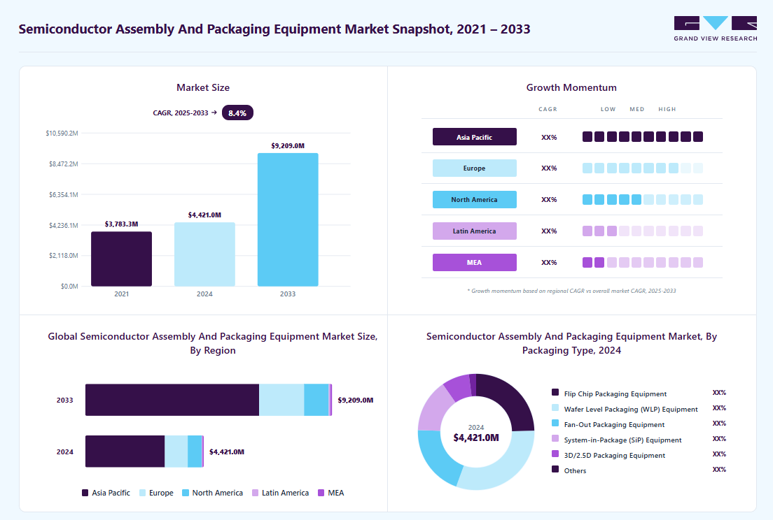
Market Size, 2024
$4,421.0MMarket Estimate, 2025
$4,816.7MMarket Forecast, 2033
$9,209.0MCAGR, 2025–2033
8.4%Semiconductor Assembly & Packaging Equipment Market Summary
The global semiconductor assembly and packaging equipment market size was estimated at USD 4,421.0 million in 2024 and is projected to reach USD 9,209.0 million by 2030, growing at a CAGR of 8.4% from 2025 to 2033. This growth is driven by rising demand for compact, high-performance electronic devices.
Key Market Trends & Insights
- Asia Pacific dominated the semiconductor assembly and packaging equipment market with the largest revenue share of 67.0% in 2024.
- The semiconductor assembly and packaging equipment market in the U.S. is expected to grow at a substantial CAGR of 6.6% from 2025 to 2033.
- By product, the packaging equipment segment is expected to grow at the fastest CAGR from 2025 to 2033.
- By packaging type, the 3D/2.5D packaging equipment segment is expected to grow at the fastest CAGR of 10.2% from 2025 to 2033.
- By end use, the OSAT (Outsourced Semiconductor Assembly and Test) segment is expected to grow at the fastest CAGR of 8.7% from 2025 to 2033.
Market Size & Forecast
- 2024 Market Size: USD 4,421.0 Million
- 2033 Projected Market Size: USD 9,209.0 Million
- CAGR (2025-2033): 8.4%
- Asia Pacific: Largest market in 2024
As consumer electronics and mobile devices become smaller yet more powerful, the need for advanced packaging technologies continues to grow to meet performance, efficiency, and miniaturization requirements. A significant driver of market growth is the increasing trend of outsourcing by fabless semiconductor companies. This shift has resulted in rising demand for assembly and packaging services provided by OSAT (Outsourced Semiconductor Assembly and Test) companies. In response, OSAT providers are heavily investing in advanced assembly and packaging equipment to meet evolving customer needs.")
In addition, government initiatives and semiconductor stimulus programs in regions such as the U.S., China, and Europe are further accelerating capital investments in chip production and packaging infrastructure. Collectively, these factors are propelling the robust growth trajectory of the semiconductor assembly and packaging equipment industry.
Market Concentration & Characteristics
The global semiconductor assembly and packaging equipment industry is moderately concentrated, with a few major players holding a significant share. Leading companies invest heavily in R&D and advanced technologies, giving them a competitive edge. However, the presence of several regional and niche players adds some degree of fragmentation. This mix creates a competitive yet innovation-driven market landscape.
The market is highly innovation-driven, with continuous advancements in packaging technologies like 3D integration, fan-out, and wafer-level packaging. Companies focus on enhancing performance, thermal efficiency, and miniaturization. Automation and AI integration in equipment design are also gaining traction. These innovations are crucial to meet the evolving demands of high-performance computing and mobile applications.

Mergers and acquisitions are fairly active in this industry as major players seek to expand technological capabilities and global reach. Larger firms often acquire niche technology providers to strengthen their position in emerging packaging formats. These deals also help accelerate product development and reduce time-to-market. M&A activity contributes to market consolidation and competitive advantage.
Regulatory frameworks around export controls, trade policies, and environmental compliance significantly impact the industry. Restrictions on semiconductor equipment exports, particularly between key markets like the U.S. and China, influence supply chains. In addition, equipment manufacturers must adhere to strict standards regarding material usage and emissions. Compliance with these regulations adds complexity and cost to operations.
Drivers, Opportunities & Restraints
The growing demand for advanced consumer electronics, including smartphones, tablets, and wearables, is a key driver of market growth. Technologies like AI, 5G, and autonomous vehicles require high-performance, compact semiconductors, boosting the need for sophisticated packaging equipment. In addition, global investments in semiconductor fabs and packaging facilities are rising, especially in the U.S., China, and South Korea. The shift toward heterogeneous integration and multi-chip packaging further accelerates equipment demand.
The market holds significant opportunities in next-generation packaging formats such as chiplet-based architectures and 3D stacking. Emerging applications in IoT, AR/VR, quantum computing, and edge AI are creating new demand for flexible, high-throughput packaging solutions. Expansion of OSAT services, especially in Southeast Asia, opens doors for equipment suppliers. Government incentives and funding under national semiconductor strategies (e.g., U.S. CHIPS Act, EU Chips Act) offer strong support for long-term growth.
The high cost of advanced packaging equipment and infrastructure poses a barrier for small and mid-sized enterprises. Complex design and integration challenges associated with newer packaging types like SiP and 3D/2.5D often slow down adoption. Geopolitical tensions, export controls, and fluctuating trade policies (notably U.S.-China relations) can impact supply chains and equipment exports. In addition, the industry faces talent shortages in areas such as semiconductor packaging design and precision engineering.
Product Insights
The bonding equipment segment led the market with the largest revenue share of 34.8% in 2024, owing to its critical role in chip interconnection processes like die bonding and wire bonding. These tools are essential for both traditional and advanced packaging formats, including flip chip and SiP. High demand from IDMs and OSATs for precision and speed has driven continuous innovation in bonding systems. The dominance is supported by widespread use across consumer electronics, automotive, and industrial applications.
The packaging equipment segment is expected to grow at the fastest CAGR of 8.7% from 2025 to 2033 in terms of revenue, owing to the increasing adoption of advanced formats such as fan-out, wafer-level, and 3D packaging. Demand for molding machines, solder plating systems, and deflashers is rising with the push for miniaturized and high-performance semiconductor packages. Growth is further fueled by the expansion of OSAT capacities and rising production volumes in Asia. Equipment manufacturers are focusing on automation and versatility to meet evolving packaging requirements.
Packaging Type Insights
The wafer level packaging equipment segment led the market with the largest revenue share of 30.9% in 2024, due to its ability to enable compact, lightweight, and high-performance chip designs, ideal for smartphones, wearables, and IoT devices. The technology allows packaging at the wafer level, reducing process steps and improving throughput. Its widespread use in high-volume consumer electronics manufacturing drives consistent demand. In addition, advancements in fan-in and fan-out WLP have expanded its application across various device categories.
3D/2.5D packaging equipment segment is expected to grow at the fastest CAGR of 10.2% from 2025 to 2033 in terms of revenue, driven by the rising need for higher performance and bandwidth in AI, HPC, and data center applications. These packaging formats support the stacking and integration of multiple dies, enabling faster data transfer and lower power consumption. As chiplet architectures gain popularity, demand for high-precision bonding and interconnect solutions is accelerating. Equipment manufacturers are investing in new tools to meet the complex alignment and thermal management needs of 3D integration.
End-use Insights
The integrated device manufacturers (IDMs) segment led the market with the largest revenue share of 55.3% in 2024, due to their in-house capabilities for both chip fabrication and packaging. They invest heavily in advanced packaging equipment like die bonders, flip chip systems, and wafer-level tools to maintain performance control and design flexibility. IDMs are early adopters of technologies such as 3D/2.5D packaging and hybrid bonding. Their vertical integration allows them to drive large-scale demand for high-end assembly equipment.

The Outsourced Semiconductor Assembly and Test (OSAT) segment is expected to grow at the fastest CAGR of 8.7% from 2025 to 2033 in terms of revenue, as fabless companies increasingly outsource packaging operations. OSATs are expanding capacities and upgrading equipment to meet rising demand for advanced packaging formats like fan-out, SiP, and WLP. The need for cost-effective, high-volume, and flexible solutions is fueling their investment in bonding, molding, and dicing tools. Their global expansion, particularly in Asia, is contributing to robust market growth.
Regional Insights
The North America semiconductor assembly and packaging equipment market is growing at a significant CAGR of 6.8% in 2024, driven by strong investments in R&D and advanced chip packaging technologies. The region is home to major IDMs and equipment manufacturers focusing on flip chip, SiP, and 3D packaging. The U.S. government’s semiconductor funding initiatives have further boosted domestic production and packaging capacity. Demand is especially strong for bonding equipment and advanced wafer-level packaging systems.
U.S. Semiconductor Assembly and Packaging Equipment Market Trends
The semiconductor assembly and packaging equipment market in the U.S. accounted for the largest market revenue share in 2024, due to its advanced semiconductor ecosystem and strong presence of IDMs and OSATs. Major investments under the CHIPS and Science Act are driving the development of cutting-edge packaging technologies like 3D/2.5D and system-in-package (SiP). Demand is high for bonding equipment, die bonders, and wafer-level packaging systems. In addition, local manufacturing expansion is strengthening domestic equipment sales.
The Canada semiconductor assembly and packaging equipment market is a growing rapidly, supported by its focus on electronics manufacturing and research collaborations in semiconductor technology. The country is witnessing gradual adoption of wafer mounting and wire bonding equipment for niche applications. Government initiatives to attract tech investments are aiding market development. Though smaller in scale, Canada’s growth is steady and driven by innovation and support infrastructure.
Europe Semiconductor Assembly and Packaging Equipment Market Trends
The semiconductor assembly and packaging equipment market in Europe is supported by its robust automotive and industrial electronics sectors, which demand high-reliability packaging. The region shows strong adoption of fan-out and 2.5D packaging technologies, especially among IDMs and specialized OSAT providers. EU-led initiatives to build semiconductor independence are encouraging capital investment in assembly equipment. Die bonders, molding machines, and solder plating systems are in high demand across key European fabs.
The Germanysemiconductor assembly and packaging equipment market is anticipated to grow at the fastest CAGR during the forecast period, driven by its strong automotive and industrial electronics sectors. The country is increasingly investing in advanced packaging technologies such as fan-out and wafer-level packaging to meet high-reliability requirements. Demand is rising for die bonders, molding equipment, and solder plating systems. Government support and public-private partnerships are further strengthening Germany semiconductor manufacturing base.
The semiconductor assembly and packaging equipment market in UK is experiencing steady growth, due to its expanding electronics and defense sectors. Investments in R&D and collaboration with European tech firms are promoting the adoption of flip chip and SiP packaging formats. Demand is increasing for precision bonding and dicing equipment in specialized applications. While the market size is smaller than Germany’s, strategic initiatives are positioning the UK for long-term growth.
Asia Pacific Semiconductor Assembly and Packaging Equipment Market Trends
The semiconductor assembly and packaging equipment market in Asia Pacific accounted for the largest market revenue share of 67.0% in 2024, owing to the concentration of leading OSATs and semiconductor manufacturing hubs in China, Taiwan, South Korea, and Japan. The region leads in high-volume adoption of dicing, wafer mounting, and wire bonding equipment. Growth is driven by the expansion of consumer electronics, 5G infrastructure, and cloud data centers. Flip chip and wafer-level packaging systems are especially prominent in high-end production lines.

The Taiwan semiconductor assembly and packaging equipment market accounted for the largest market revenue share of 35.3% in Asia Pacific in 2024, driven by its robust semiconductor and electronics manufacturing sectors. These industries require precise and efficient cooling solutions to maintain optimal production conditions. Investments in green factories and energy-efficient infrastructure boost demand for modern cooling towers. Government initiatives supporting sustainable industrial practices further strengthen market growth.
The semiconductor assembly and packaging equipment market in China is the key player in Asia Pacific region, driven by strong government support and increasing domestic chip production. The country is heavily investing in OSAT capabilities and adopting advanced packaging formats such as wafer-level and 3D packaging. Demand is particularly high for dicing equipment, die bonders, and molding machines to support high-volume manufacturing. Geopolitical pressures and import restrictions are also driving efforts to localize equipment production.
Middle East & Africa Semiconductor Assembly and Packaging Equipment Market Trends
The semiconductor assembly and packaging equipment market in Middle East and Africa are in the early stages of semiconductor ecosystem development but show growing interest due to diversification strategies. Government-backed initiatives are promoting investments in tech and electronics assembly infrastructure. The demand for basic packaging and mounting equipment is slowly increasing. Long-term growth potential lies in supporting global supply chain resilience and localized electronics production.
The Israel semiconductor assembly and packaging equipment market is emerging as a growing player in MEA region, driven by its strong R&D capabilities and high-tech innovation ecosystem. The country is investing in advanced chip packaging technologies to support its thriving defense, telecommunications, and AI sectors. Demand is increasing for precision bonding, flip chip, and system-in-package (SiP) equipment. Strategic collaborations with global semiconductor companies are further accelerating technology adoption and market growth.
Latin America Semiconductor Assembly and Packaging Equipment Market Trends
The semiconductor assembly and packaging equipment market in Latin America is emerging as a growing market due to increasing investments in electronics manufacturing. Although it lacks major IDM or OSAT hubs, the region is gradually adopting advanced packaging processes in support roles. Equipment demand is rising for wire bonders and entry-level dicing systems. Growth is expected to be moderate but steady as regional supply chains develop.
The Brazil semiconductor assembly and packaging equipment market is witnessing gradual growth, driven by increasing investments in electronics manufacturing. The government is supporting local production through tax incentives and technology development programs. Demand is rising for entry-level dicing, wire bonding, and wafer mounting equipment to support regional assembly operations. Brazil’s growing consumer electronics and automotive sectors are further boosting market potential.
Semiconductor Assembly And Packaging Equipment Company Insight
Some of the key players operating in the market include Applied Materials, ASM Pacific Technology, Veeco Instruments Inc.
-
Applied Materials is a supplier of advanced packaging equipment, particularly focused on enabling next-generation chip architectures through technologies like hybrid bonding and wafer-level integration. The company plays a critical role in the evolution of heterogeneous integration and 3D stacking, supporting the performance demands of AI, data centers, and high-performance computing. Its integrated material solutions bridge front-end wafer fabrication and back-end packaging, optimizing interconnect density and power efficiency. Applied Materials also invests heavily in packaging R&D, often collaborating with major IDMs and OSATs to push the limits of system scaling.
-
ASM Pacific Technology focuses heavily on advanced packaging solutions, including fan-out, flip chip, and system-in-package (SiP) technologies tailored for high-density applications. The company delivers precision bonding systems and automation platforms widely adopted by major OSATs and IDMs. It also leads in developing integrated hardware-software solutions to enhance packaging throughput and yield. ASMPT’s innovations directly support miniaturization and heterogeneous integration in next-generation semiconductor devices.
Key Semiconductor Assembly And Packaging Equipment Companies:
The following are the leading companies in the semiconductor assembly and packaging equipment market. These companies collectively hold the largest market share and dictate industry trends.
- Applied Materials
- ASM Pacific Technology
- Veeco Instruments Inc.
- Besi
- Disco Corporation
- Kulicke & Soffa Industries, Inc. (K&S)
- Lam Research Corporation
- Nikon Corporation
- Plasma-Therm
- Rudolph Technologies, Inc.
- SCREEN Semiconductor Solutions Co., Ltd.
- SUSS MicroTec SE
- Teradyne, Inc.
- Tokyo Electron Limited (TEL)
- Ultratech, Inc.
Recent Developments
-
In May 2025, Veeco announced receiving over USD 35 million in orders for its AP300 advanced packaging lithography systems from both IDMs and OSATs. These systems will support expanding production needs tied to AI and high-performance computing markets. The AP300 is optimized for applications like copper pillar bumping, flip chip, and fan-out wafer-level packaging. This order boost is expected to strengthen Veeco’s advanced packaging equipment business significantly in 2025.
-
In August 2024, Polymatech, an Indian opto-semiconductor firm, acquired U.S.-based Nisene Technology Group to strengthen its presence in IC packaging and testing. The move supports Polymatech’s goal of building a comprehensive semiconductor ecosystem. It also includes plans for major investment to expand operations in the U.S. This acquisition boosts the company’s capabilities across the chipmaking value chain.
-
In November 2022, Lam Research acquired SEMSYSCO to bolster its advanced packaging capabilities in semiconductor manufacturing. The acquisition enhances its wet processing and panel-level packaging technology for seamless integration in next-generation chip designs. This strategic move is aimed at strengthening its solutions for high-performance computing and AI applications. The deal marks a significant expansion of Lam Research’s portfolio in the advanced packaging ecosystem.
Semiconductor Assembly & Packaging Equipment Market Report Scope
Report Attribute
Details
Market size value in 2025
USD 4,816.7 million
Revenue forecast in 2033
USD 9,209.0 million
Growth rate
CAGR of 8.4% from 2025 to 2033
Base year for estimation
2024
Historical data
2021 - 2023
Forecast period
2025 - 2033
Quantitative units
Revenue in USD million/billion, and CAGR from 2025 to 2033
Report coverage
Revenue forecast, company ranking, competitive landscape, growth factors, and trends
Segments covered
Product, end-use, packaging type, region.
Regional scope
North America; Europe; Asia Pacific; Latin America; Middle East & Africa
Country scope
U.S.; Canada; Mexico; UK; Germany; France; Spain;Netherlands; Italy; China; Japan; India; Taiwan; South Korea; Brazil; South Africa; Israel
Key companies profiled
Applied Materials; ASM Pacific Technology; Veeco Instruments Inc.; Besi; Disco Corporation; Kulicke & Soffa Industries, Inc. (K&S); Lam Research Corporation; Nikon Corporation; Plasma-Therm; Rudolph Technologies, Inc.; SCREEN Semiconductor Solutions Co., Ltd.; SUSS MicroTec SE; Teradyne, Inc.; Tokyo Electron Limited (TEL); Ultratech, Inc.
Customization scope
Free report customization (equivalent up to 8 analysts working days) with purchase. Addition or alteration to country, regional & segment scope.
Pricing and purchase options
Avail customized purchase options to meet your exact research needs. Explore purchase options
Global Semiconductor Assembly & Packaging Equipment Market Report Segmentation
This report forecasts revenue growth at global, regional, and country levels and provides an analysis of the latest industry trends in each of the sub-segments from 2021 to 2033. For this study, Grand View Research has segmented the global semiconductor assembly and packaging equipment market report based on packaging type,end-use, product and region.

-
Packaging Type Outlook (Revenue, USD Million, 2021 - 2033)
-
Flip Chip Packaging Equipment
-
Wafer Level Packaging (WLP) Equipment
-
Fan-Out Packaging Equipment
-
System-in-Package (SiP) Equipment
-
3D/2.5D Packaging Equipment
-
Others
-
-
End-use Outlook (Revenue, USD Million, 2021 - 2033)
-
IDMs (Integrated Device Manufacturers)
-
OSAT (Outsourced Semiconductor Assembly and Test)
-
-
Product Outlook (Revenue, USD Million, 2021 - 2033)
-
Dicing Equipment
-
Scriber
-
Dicer
-
Wafer Mounting Equipment
-
-
Bonding Equipment
-
Die Bonder
-
Wire Bonder
-
Others
-
-
Packaging Equipment
-
Molding Equipment
-
Solder Plating Equipment
-
Deflasher
-
Others
-
-
Others
-
-
Regional Outlook (Revenue, USD Million, 2021 - 2033)
-
North America
-
U.S.
-
Canada
-
-
Mexico
-
Europe
-
Germany
-
France
-
Italy
-
Spain
-
UK
-
Netherlands
-
-
Asia Pacific
-
China
-
India
-
Japan
-
South Korea
-
Taiwan
-
-
Latin America
-
Brazil
-
-
Middle East and Africa
-
Israel
-
South Africa
-
-
Frequently Asked Questions About This Report
The global semiconductor assembly and packaging equipment market size was estimated at USD 4,421.0 million in 2024 and is expected to be USD 4,816.7 million in 2025.
The global semiconductor assembly and packaging equipment market, in terms of revenue, is expected to grow at a compound annual growth rate of 8.4% from 2025 to 2033 to reach USD 9,209.0 million by 2033.
Which segment accounted for the largest semiconductor assembly and packaging equipment market share?Integrated Device Manufacturers (IDMs) segment accounted for a share of 55.3% in 2024, due to their in-house capabilities for both chip fabrication and packaging. They invest heavily in advanced packaging equipment like die bonders, flip chip systems, and wafer-level tools to maintain performance control and design flexibility.
Some of the key players operating in the global semiconductor assembly and packaging equipment market include Applied Materials; ASM Pacific Technology; Veeco Instruments Inc.; Besi; Disco Corporation; Kulicke & Soffa Industries, Inc. (K&S); Lam Research Corporation; Nikon Corporation; Plasma-Therm; Rudolph Technologies, Inc.; SCREEN Semiconductor Solutions Co., Ltd.; SUSS MicroTec SE; Teradyne, Inc.; Tokyo Electron Limited (TEL); Ultratech, Inc.
Key factors driving the global semiconductor assembly and packaging equipment market include the growing demand for compact, high-performance electronic devices, increased outsourcing by fabless semiconductor companies to OSAT providers, and rising investments in advanced packaging technologies.
About the Author(s)
Advanced Interior Materials Research Team
Advanced Materials · Advanced Interior MaterialsThis report was authored by the advanced interior materials research team at Grand View Research - comprising two research analysts, one senior research analyst, and one industry expert - with specialized expertise in the advanced interior materials segment of the advanced materials industry. All findings are based on proprietary advanced materials databases, executive interviews, and regulatory analysis, subject to internal peer review prior to publication.
Last Updated:
Speak to Analyst


Share this report with your colleague or friend.
Need a Tailored Report?
Customize this report to your needs — add regions, segments, or data points, with 20% free customization.

ISO 9001:2015 & 27001:2022 Certified
We are GDPR and CCPA compliant! Your transaction & personal information is safe and secure. For more details, please read our privacy policy.