- Home
- »
- Advanced Interior Materials
- »
-
U.S. Semiconductor Defect Inspection Equipment Market Report, 2033GVR Report cover
![U.S. Semiconductor Defect Inspection Equipment Market Size, Share & Trends Report]()
U.S. Semiconductor Defect Inspection Equipment Market (2025 - 2033) Size, Share & Trends Analysis Report By Defect Type (Crystal Defect Inspection, Mask/Reticle Defect Inspection), By Technology, By Process Stage, By Inspection Technique, By End Use, And Segment Forecasts
- Report ID: GVR-4-68040-680-3
- Number of Report Pages: 100
- Format: PDF
- Historical Range: 2021 - 2023
- Forecast Period: 2025 - 2033
- Industry: Advanced Materials
- Report Summary
- Table of Contents
- Segmentation
- Methodology
- Download FREE Sample
-
Download Sample Report
Market Size & Trends
The U.S. semiconductor defect inspection equipment market size was valued at USD 558.5 million in 2024 and is projected to grow at a CAGR of 7.2% from 2025 to 2033. The rapid evolution of semiconductor applications in areas such as AI, 5G, and electric vehicles is fueling the demand for precise defect inspection solutions.
Key Market Trends & Insights
- The semiconductor defect inspection equipment market in the U.S. is expected to grow at a CAGR of 7.2% from 2025 to 2033.
- By defect type, the metal defect inspection segment is expected to grow at a considerable CAGR of 7.9% from 2025 to 2033 in terms of revenue.
- By technology, the optical inspection segment is expected to grow at a considerable CAGR of 7.6% from 2025 to 2033 in terms of revenue.
- By end use, the foundry segment is expected to grow at a considerable CAGR of 8.0% from 2025 to 2033 in terms of revenue.
Market Size & Forecast
- 2024 Market Size: USD 558.5 Million
- 2033 Projected Market Size: USD 1,019.5 Million
- CAGR (2025-2033): 7.2%
These cutting-edge technologies rely on ultra-small nodes, making early defect detection vital for maintaining yield and reliability. Another significant driver is the U.S. government’s emphasis on domestic semiconductor manufacturing through initiatives like the CHIPS Act. With increased funding for fabrication facilities, there is a corresponding rise in demand for inspection equipment to maintain production quality and compliance. Furthermore, the integration of machine learning and advanced analytics in inspection systems is enhancing defect detection accuracy. This technological edge is attracting major players to scale up operations within the U.S. semiconductor ecosystem.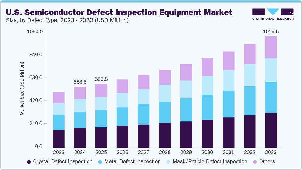
Market Concentration & Characteristics
The industry is highly concentrated, with a few major players dominating the landscape. Some companies hold significant market share due to their advanced technologies and established client base. High entry barriers, such as capital intensity, technical complexity, and long customer qualification cycles, limit new entrants. As a result, competition remains limited, reinforcing the dominance of top-tier firms.
The industry is characterized by a high degree of innovation driven by the push toward smaller process nodes and advanced packaging. Companies invest heavily in R&D to improve detection accuracy and speed using AI, deep learning, and high-resolution imaging. Innovation is crucial for staying competitive, especially with rapid changes in chip architectures. Continuous product upgrades are essential to meet the evolving demands of U.S. chip manufacturers.
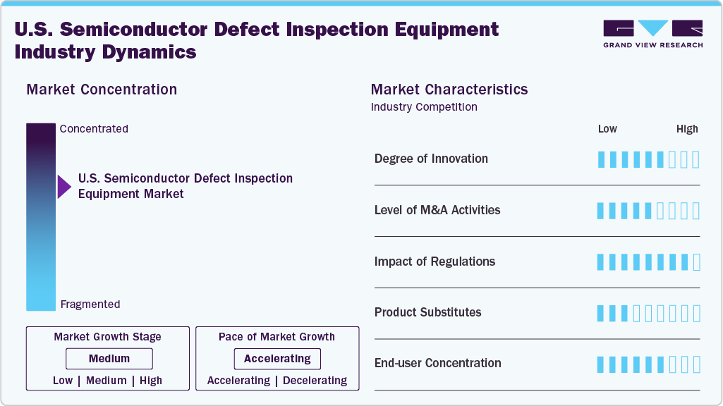
Mergers and acquisitions are moderately active in the U.S. market, primarily aimed at expanding technological capabilities and product portfolios. Leading companies often acquire smaller firms with niche technologies to enhance inspection accuracy or automation. These deals are also driven by the need to consolidate resources and strengthen domestic supply chains. Strategic M&A plays a role in maintaining competitiveness amid global supply chain shifts.
Regulation plays a growing role in shaping the U.S. market, especially with government efforts to localize semiconductor production. Policies under the CHIPS and Science Act encourage domestic manufacturing and indirectly boost demand for defect inspection tools. Export control regulations also impact the industry by restricting the sale of advanced equipment to certain countries. Overall, compliance with national security and trade laws has become critical for U.S.-based equipment vendors.
Drivers, Opportunities & Restraints
The market is driven by the increasing demand for high-performance chips in AI, automotive, and 5G applications. As devices shrink in size, detecting microscopic defects becomes more critical to ensure yield and reliability. Government initiatives like the CHIPS Act are boosting local semiconductor manufacturing and driving equipment demand. Continuous R&D investments by key players also fuel innovation and market growth.
Emerging technologies such as quantum computing, advanced packaging, and EUV lithography create new opportunities for defect inspection tools. The reshoring of semiconductor production to the U.S. opens up fresh demand for inspection systems across new fabs. Integration of AI and machine learning in inspection processes offers potential for smarter, faster defect analysis. Collaborations with national labs and research centers further support long-term growth prospects.
High capital costs and long equipment development cycles can hinder new entrants and delay technology adoption. The complexity of integrating inspection tools with evolving semiconductor processes poses additional challenges. Geopolitical tensions and export restrictions may disrupt global supply chains and access to advanced components. Moreover, dependence on a few dominant vendors limits market competition and flexibility for buyers.
Defect Type Insights
The crystal defect inspection segment dominated the market and accounted for a share of 32.6% in 2024, due to its critical role in early-stage wafer quality control. These defects, if undetected, can compromise the entire chip manufacturing process and reduce yield. As semiconductor nodes shrink, the demand for precise crystal integrity checks increases. U.S. fabs rely heavily on advanced tools to ensure defect-free substrates for high-performance applications.
Metal defect inspection is the fastest-growing segment, driven by the increasing complexity of interconnect structures in advanced semiconductor designs. As devices scale down, even minute metal impurities can lead to short circuits or performance issues. The rise of multi-layered chips and 3D packaging further amplifies the need for accurate metal defect detection. This trend is pushing U.S. manufacturers to invest in high-resolution inspection technologies.
Technology Insights
The optical inspection segment accounted for a share of 35.4% in 2024 owing to its speed, cost-effectiveness, and ability to handle high-throughput production lines. It is widely used for detecting surface-level defects during various stages of wafer processing. Its non-destructive nature and compatibility with existing fab workflows make it the preferred choice for most manufacturers. Continued enhancements in resolution and automation have further solidified its dominance.
Electron beam inspection is growing rapidly due to its superior resolution and ability to detect ultra-small and buried defects. As semiconductor nodes reach sub-5nm scales, optical methods alone become insufficient for critical dimension inspection. E-beam systems provide detailed analysis essential for advanced logic and memory devices. This makes them increasingly vital in U.S. fabs adopting next-generation chip technologies.
Process Stage Insights
Front-End of Line (FEOL) dominated the market and accounted for a 43.5% share in 2024, as it involves the initial and most critical stages of chip fabrication. Defects in this stage can severely impact device performance, making inspection essential for quality assurance. High precision tools are required to monitor processes like photolithography, doping, and etching. The growing complexity of transistor architectures further reinforces the need for robust FEOL inspection solutions.
Packaging and assembly is the fastest growing segment due to the rise of advanced packaging technologies such as 2.5D, 3D ICs, and chiplet integration. These innovations demand highly accurate inspection to detect interconnect, bonding, and delamination defects. As performance and miniaturization needs increase, packaging plays a more critical role in overall chip functionality. U.S. manufacturers are rapidly adopting new inspection tools to ensure reliability in complex package designs.
Inspection Technique Insights
The 3D inspection techniques segment accounted for a share of 43.9% in 2024,owing to their ability to accurately detect defects in complex, multi-layered structures. These techniques are essential for advanced nodes and packaging technologies where traditional 2D methods fall short. They enable precise imaging of surface and subsurface features, ensuring better process control. The growing adoption of 3D NAND and 3D ICs has further accelerated the use of 3D inspection tools.
Machine learning and AI-based inspection is the fastest growing segment, driven by the need for faster and more intelligent defect detection in high-volume production. These technologies enhance pattern recognition, anomaly detection, and decision-making, reducing false positives and inspection time. As chips become more complex, AI helps adapt inspection parameters in real time for higher accuracy. U.S. fabs are increasingly investing in AI-integrated systems to improve efficiency and yield outcomes.
End Use Insights
The foundry segment accounted for a share of 31.5% in 2024 due to its high production volumes and diverse customer base. These facilities require advanced inspection tools to ensure consistent quality across multiple product lines and technologies. With increasing demand for custom chips in AI and consumer electronics, foundries invest heavily in defect detection. Their focus on efficiency and yield optimization makes them key users of cutting-edge inspection solutions.
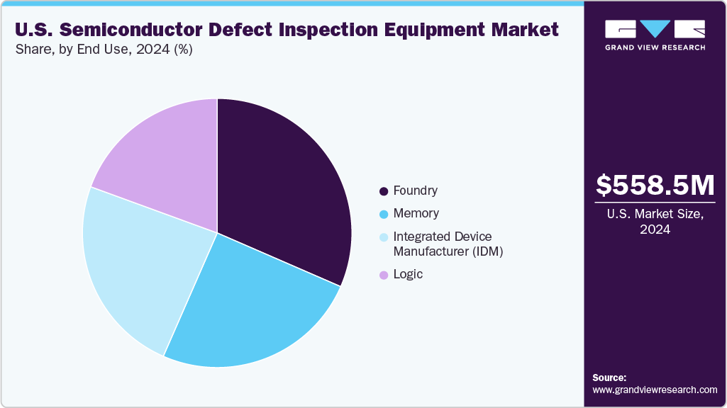
Integrated Device Manufacturers (IDMs) are growing significantly as they expand in-house production capabilities to reduce dependency on external suppliers. Supported by U.S. government incentives, many IDMs are building new fabs and upgrading existing ones. This shift drives demand for defect inspection tools to ensure quality across design, fabrication, and packaging. As IDMs adopt advanced nodes and packaging technologies, inspection becomes increasingly critical to maintain performance standards.
Key U.S. Semiconductor Defect Inspection Equipment Companies Insights
Key players operating in the U.S. semiconductor defect inspection equipment market are undertaking various initiatives to strengthen their presence and increase the reach of their products and services. Strategies such as expansion activities and partnerships are key in propelling the market growth.
Key U.S. Semiconductor Defect Inspection Equipment Companies:
- Merck KGaA
- KLA Corporation
- Toray Group
- PDF Solutions
- Hitachi High-Tech Corporation
- Camtek
- Onto Innovation
- HORIBA Group
- Applied Materials, Inc.
- Komatsu NTC.
Recent Developments
-
In February 2025, Toray Engineering’s subsidiary, TASMIT, launched a new inspection system under its INSPECTRA series, tailored for large glass substrates used in advanced semiconductor packaging. It is the first in the industry to inspect both surfaces and internal layers of 650 mm square glass interposers. The system enables high-speed inspection, processing each panel in approximately 40 seconds. Shipments will begin in March 2025, with ambitious sales targets set for the coming years.
-
In July 2024, Merck KGaA, Darmstadt, Germany, announced the acquisition of Unity SC to strengthen its capabilities in semiconductor inspection and metrology. Unity SC specializes in advanced 3D inspection and metrology tools used in hybrid bonding, 3D stacking, and compound semiconductors. The move supports Merck’s strategy to expand its electronics portfolio and cater to AI and HPC semiconductor markets. The transaction is expected to close by the end of 2024, pending regulatory approvals.
U.S. Semiconductor Defect Inspection Equipment Market Report Scope
Report Attribute
Details
Market size value in 2025
USD 585.8 million
Revenue forecast in 2033
USD 1,019.5 million
Growth rate
CAGR of 7.2% from 2025 to 2033
Historical data
2021 - 2023
Forecast period
2025 - 2033
Quantitative units
Revenue in USD million/billion and CAGR from 2025 to 2033
Report coverage
Revenue forecast, company ranking, competitive landscape, growth factors, and trends
Segments covered
Defect type, technology, process stage, inspection technique, end use
Country scope
U.S.
Key companies profiled
Merck KGaA; KLA Corporation; Toray Group; PDF Solutions; Hitachi High-Tech Corporation; Camtek; Onto Innovation; HORIBA Group; Applied Materials, Inc.; Komatsu NTC.
Customization scope
Free report customization (equivalent up to 8 analysts working days) with purchase. Addition or alteration to country, regional & segment scope.
Pricing and purchase options
Avail customized purchase options to meet your exact research needs. Explore purchase options
U.S. Semiconductor Defect Inspection Equipment Market Report Segmentation
This report forecasts revenue growth at the U.S. level and provides an analysis of the latest industry trends in each of the sub-segments from 2021 to 2033. For this study, Grand View Research has segmented the U.S. semiconductor defect inspection equipment market report based on defect type, technology, process stage, inspection technique, and end use.
-
Defect Type Outlook (Revenue, USD Million, 2021 - 2033)
-
Crystal Defect Inspection
-
Metal Defect Inspection
-
Mask/Reticle Defect Inspection
-
Others
-
-
Technology Outlook (Revenue, USD Million, 2021 - 2033)
-
Optical Inspection
-
Electron Beam Inspection
-
X-ray Inspection
-
Others
-
-
Inspection Technique Outlook (Revenue, USD Million, 2021 - 2033)
-
2D Inspection Techniques
-
3D Inspection Techniques
-
Machine Learning and AI
-
-
Process Stage Outlook (Revenue, USD Million, 2021 - 2033)
-
Front-End of Line (FEOL)
-
Back-End of Line (BEOL)
-
Photomask Shops / Reticle Inspection
-
Packaging & Assembly
-
R&D and Failure Analysis
-
-
End Use Outlook (Revenue, USD Million, 2021 - 2033)
-
Foundry
-
Memory
-
Logic
-
Integrated Device Manufacturer (IDM)
-
Frequently Asked Questions About This Report
b. The U.S. semiconductor defect inspection equipment market size was estimated at USD 558.5 million in 2024 and is expected to be USD 585.8 million in 2025.
b. The U.S. HVAC filtration market, in terms of revenue, is expected to grow at a compound annual growth rate of 7.2% from 2025 to 2033 to reach USD 1,019.5 million by 2033.
Which segment accounted for the largest U.S. semiconductor defect inspection equipment market share?b. Crystal defect inspection segment dominated the market and accounted for a share of 32.6% in 2024, due to its critical role in early-stage wafer quality control. These defects, if undetected, can compromise the entire chip manufacturing process and reduce yield. As semiconductor nodes shrink, the demand for precise crystal integrity checks increases.
b. Some of the key players operating in the U.S. semiconductor defect inspection equipment market include Merck KGaA; KLA Corporation; Toray Group; PDF Solutions; Hitachi High-Tech Corporation; Camtek; Onto Innovation; HORIBA Group; Applied Materials, Inc.; Komatsu NTC.
b. Key factors driving the U.S. semiconductor defect inspection equipment market include the push for advanced chip manufacturing and the expansion of domestic fabs supported by government initiatives. Rising complexity in semiconductor designs and the need for high yield further boost demand for precision inspection tools.
Share this report with your colleague or friend.
Need a Tailored Report?
Customize this report to your needs — add regions, segments, or data points, with 20% free customization.

ISO 9001:2015 & 27001:2022 Certified
We are GDPR and CCPA compliant! Your transaction & personal information is safe and secure. For more details, please read our privacy policy.
Trusted market insights - try a free sample
See how our reports are structured and why industry leaders rely on Grand View Research. Get a free sample or ask us to tailor this report to your needs.


