- Home
- »
- Advanced Interior Materials
- »
-
Semiconductor Ceramics Market Size Report, 2026-2033GVR Report cover
![Semiconductor Ceramics Market (2026 - 2033)Report]()
Semiconductor Ceramics Market (2026 - 2033)
Size, Share & Trends Analysis Report By End-use (Logic Semiconductor Chips, Memory, Power Semiconductor), By Material (Alumina, Aluminum Nitride, Silicon Carbide, Silicon Nitride), By Region, And Segment Forecasts
Market Size, 2025
$10.0BMarket Estimate, 2026
$10.7BMarket Forecast, 2033
$16.7BCAGR, 2026–2033
6.5%Semiconductor Ceramics Market Summary
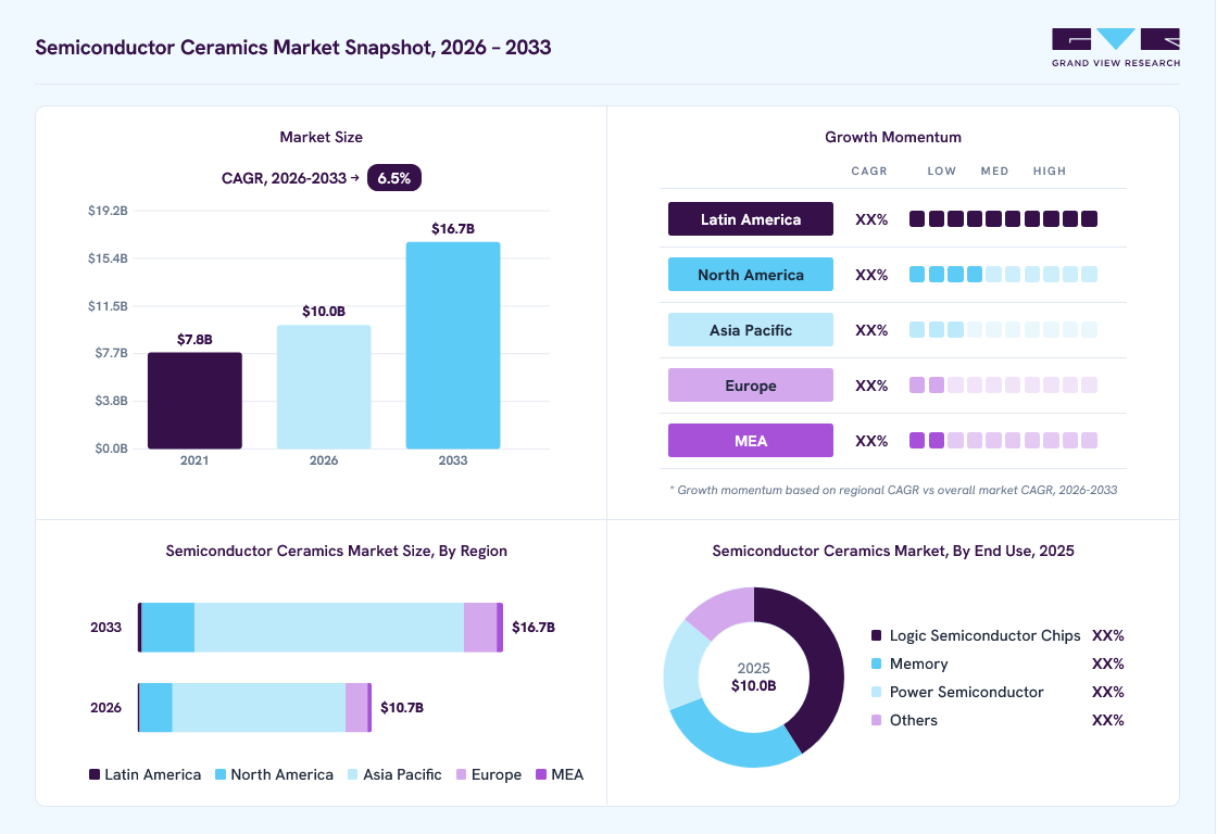
The global semiconductor ceramics market size was estimated at USD 10.0 billion in 2025 and is projected to grow from USD 10.7 billion in 2026 to USD 16.7 billion by 2033, registering a CAGR of 6.5% from 2026 to 2033. Asia Pacific dominated the semiconductor ceramics market with the largest revenue share of 73.9% in 2025. Semiconductor ceramics are strategically important to advanced chip production because they enable contamination control, plasma resistance, thermal management, and precision performance across fabrication equipment, AI chips, high-performance computing devices, and advanced packaging applications.
Key Market Trends & Insights
- By end use: Logic semiconductor chips accounted for the largest market revenue share of 41.4% in 2025.
- By material: Aluminum nitride segment is anticipated to register the fastest CAGR of 6.9% from 2026 to 2033.
Regional Highlights
- Largest Market Region in 2025: Asia Pacific (73.9% market revenue share, 2025)
- Fastest-growing market region: North America (highest CAGR, 2026 - 2033)
- By Country: China held the largest revenue share in 2025
Market Size & Forecast
- Market size in 2025: USD 10.0 billion
- Estimated market size in 2026: USD 10.7 billion
- Projected market size by 2033: USD 16.7 billion
- CAGR (2026-2033): 6.5%
Semiconductor ceramics are essential advanced engineering materials for wafer fabrication equipment and electronic packaging, where high thermal stability, electrical insulation, plasma resistance, chemical inertness, and mechanical strength are required. Materials such as alumina, aluminum nitride, silicon carbide, silicon nitride, yttria, quartz, and zirconia are used in electrostatic chucks, chamber liners, focus rings, ceramic heaters, wafer carriers, and related substrates.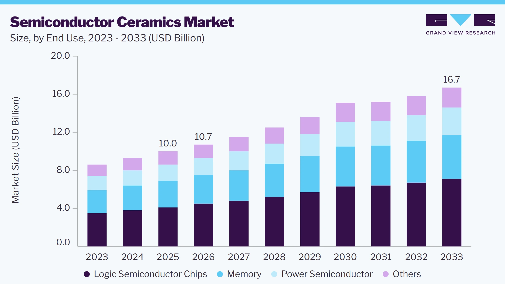
As manufacturers adopt smaller process nodes, larger wafer sizes, and advanced packaging technologies, the demand for high-purity ceramic components continues to increase. Growing investments in semiconductor fabrication facilities across the Asia Pacific, North America, and Europe are further supporting market growth.
Market Dynamics
The rapid expansion of semiconductor fabrication capacity is a key driver of the market. Rising demand for artificial intelligence (AI), high-performance computing (HPC), 5G infrastructure, electric vehicles, and advanced consumer electronics has accelerated investments in new wafer fabrication plants and capacity expansions worldwide. Since they offer excellent plasma resistance, thermal management, and dimensional stability, they are critical for ensuring precision and contamination-free chip manufacturing processes.
Government initiatives aimed at strengthening domestic semiconductor production are further supporting market growth. Programs such as the U.S. CHIPS and Science Act, the European Chips Act, and significant investments across China, Japan, South Korea, and Taiwan are driving the installation of advanced semiconductor manufacturing equipment. As fabrication technologies continue to evolve toward sub-3 nm process nodes, the need for high-performance ceramic components with superior purity and durability is expected to grow steadily.
The manufacturing of this requires ultra-high-purity raw materials, precision machining, advanced sintering technologies, and rigorous quality control, making production significantly more expensive than conventional ceramics. Components must meet extremely tight dimensional tolerances and contamination standards, as even minor defects can negatively impact semiconductor fabrication yields and equipment reliability.
The machining of hard ceramic materials into complex geometries demands specialized equipment and technical expertise, resulting in longer production cycles and higher capital investment. Limited availability of qualified manufacturers capable of producing high-performance components further increases procurement costs, posing a challenge for smaller equipment manufacturers and emerging fabrication facilities.
The growing adoption of advanced semiconductor packaging technologies, including 2.5D/3D packaging, chiplet architectures, and heterogeneous integration, presents significant growth opportunities for the market. These technologies require highly reliable ceramic substrates and precision-engineered components capable of delivering superior thermal management, electrical insulation, and dimensional stability. Furthermore, increasing investments in AI processors, high-bandwidth memory (HBM), and next-generation data center chips are driving demand for advanced semiconductor manufacturing equipment, creating long-term opportunities for manufacturers of high-performance ceramic materials and components.
Analyst Perspective
The semiconductor ceramics market is poised for steady long-term growth, driven by rising investments in semiconductor fabrication and increasing demand for AI, high-performance computing, and advanced packaging technologies. The transition to smaller process nodes and larger wafer sizes is boosting demand for high-purity ceramic components. Advancements in ceramic materials and precision manufacturing are improving process efficiency and reducing contamination. These trends are expected to support sustained market expansion over the forecast period.
End Use Insights
The logic semiconductor chips segment accounted for the largest share of the market, representing 41.4% of total revenue in 2025, and is also projected to register the highest CAGR of 6.8% during the forecast period. The segment's dominance is driven by the rapid growth in artificial intelligence (AI), high-performance computing (HPC), cloud data centers, and 5G infrastructure, all of which require advanced logic devices manufactured using highly sophisticated wafer fabrication processes.
The memory segment is expected to witness steady growth over the forecast period, supported by increasing demand for DRAM, NAND Flash, and high-bandwidth memory (HBM) used in AI servers, smartphones, consumer electronics, and enterprise storage systems. Rising investments in advanced memory fabrication facilities and the transition toward higher-density memory architectures are driving the adoption of high-performance ceramic components in wafer processing and packaging equipment. The growing deployment of AI infrastructure and data centers is expected further to strengthen demand for it across memory manufacturing applications.
Material Insights
Alumina accounted for the largest share of 37.7% in 2025, owing to its excellent electrical insulation, high mechanical strength, chemical resistance, and cost-effectiveness. It is extensively used in electrostatic chucks, chamber liners, insulators, wafer carriers, and other semiconductor processing components where high purity and dimensional stability are critical. Its broad compatibility with semiconductor manufacturing equipment and relatively lower production cost continue to support its dominant market position.
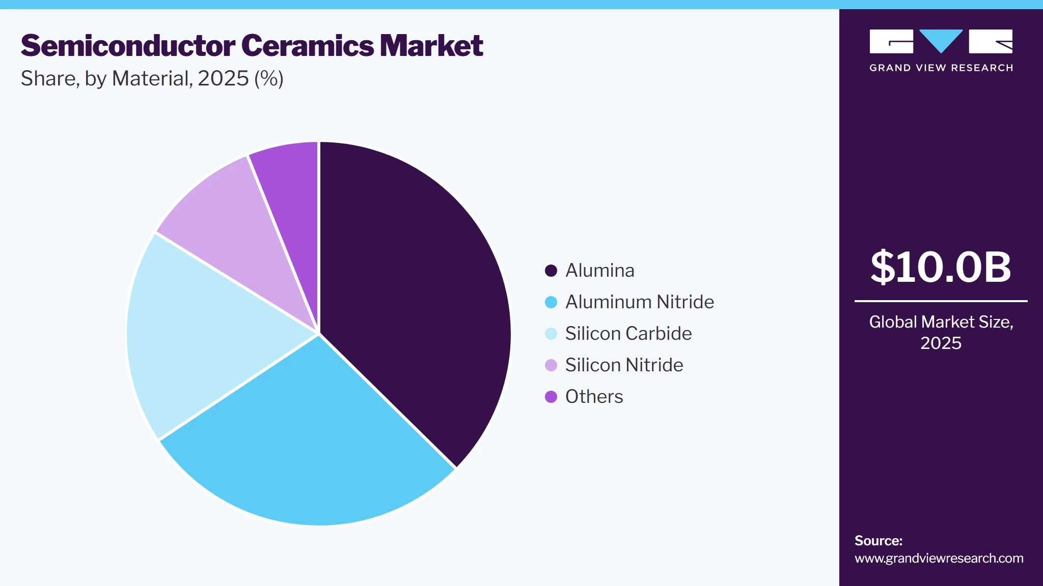
The aluminum nitride segment is projected to register the highest CAGR of 6.9% during the forecast period. Its exceptional thermal conductivity, combined with excellent electrical insulation, makes it an ideal material for ceramic substrates, packaging, ceramic heaters, and thermal management components used in advanced chip manufacturing. Increasing demand for AI processors, high-power devices, and advanced packaging technologies is expected to accelerate the adoption of aluminum nitride ceramics in next-generation fabrication.
Regional Insights
Asia Pacific dominated the global market in 2025 and is expected to maintain its leading position throughout the forecast period. The region is home to major semiconductor manufacturing hubs, including China, Taiwan, South Korea, Japan, and Singapore, where continuous investments in wafer fabrication plants and advanced chip production are driving demand for high-performance ceramic materials. Strong government support, expanding electronics manufacturing, and increasing production of AI, memory, and logic chips continue to reinforce the region's market leadership.

China is expected to remain the largest market in the Asia Pacific region, driven by substantial investments in domestic manufacturing and government initiatives to strengthen the local supply chain. The expansion of wafer fabrication facilities, advanced packaging plants, and equipment manufacturing is increasing demand for high-purity ceramic components used in etching, deposition, and lithography. Rising production of AI, memory, and logic, coupled with growing investments under China's semiconductor self-sufficiency strategy, is expected to sustain demand for it throughout the forecast period.
Europe Semiconductor Ceramics Market Trends
Europe represents a steadily growing market, driven by the European Chips Act and increasing investments in its manufacturing and R&D. Countries such as Germany, France, the Netherlands, and Ireland are expanding capabilities in automotive, industrial electronics, and power devices. The presence of leading semiconductor equipment manufacturers and advanced ceramic material producers is further supporting demand for precision-engineered ceramic components across fabrication and packaging applications.
North America Semiconductor Ceramics Market Trends
North America is expected to account for a significant share of the market, supported by strong investments in domestic manufacturing and advanced research activities. Government initiatives such as the U.S. CHIPS and Science Act are accelerating the construction and expansion of fabrication facilities, driving demand for high-performance ceramic components. The region also benefits from the presence of leading equipment manufacturers, advanced materials suppliers, and research institutions focused on next-generation chip technologies.
U.S. Semiconductor Ceramics Market Trends
The U.S. dominated the North American market owing to substantial investments in fabrication, AI processors, defense electronics, and high-performance computing. Major chip manufacturers and equipment suppliers continue to expand production capacity, increasing the demand for plasma-resistant and high-purity ceramic components used in wafer processing equipment. Government funding for domestic manufacturing and the growing adoption of advanced packaging technologies are expected to strengthen market growth further.
Latin America Semiconductor Ceramics Market Trends
The Latin American market is expected to witness moderate growth, supported by increasing investments in electronics manufacturing and the gradual development of regional supply chains. Countries such as Brazil and Mexico are strengthening their electronics and automotive manufacturing sectors, creating demand for semiconductor components and related production equipment. Although fabrication capacity remains limited, expanding industrial automation and government initiatives to attract high-tech investments are expected to support future market growth.
Middle East & Africa Semiconductor Ceramics Market Trends
The Middle East & Africa market is anticipated to grow at a steady pace, driven by increasing investments in technology infrastructure, digital transformation, and electronics manufacturing. Countries including the UAE, Saudi Arabia, and Israel are investing in research, advanced manufacturing, and data center development to diversify their economies. While the region has a relatively small semiconductor manufacturing base, rising adoption of advanced electronics and government initiatives supporting high-tech industries are expected to create new opportunities for its component suppliers.
Key Semiconductor Ceramics Company Insights
Some of the key players operating in the market include Kyocera Corporation, CoorsTek, Inc., and others.
-
Kyocera Corporation is a global manufacturer of advanced ceramics, electronic components, semiconductor packages, and industrial solutions, serving the semiconductor, automotive, telecommunications, and industrial sectors. The company's offerings in the semiconductor ceramics market include alumina and aluminum nitride ceramic substrates, ceramic packages, electrostatic chucks, ceramic heaters, wafer processing components, and high-purity ceramic parts for semiconductor manufacturing equipment.
-
CoorsTek, Inc. is a leading global manufacturer of engineered technical ceramics, supplying high-performance ceramic materials and precision components for semiconductor, medical, aerospace, and industrial applications. The company's offerings in the semiconductor ceramics market include high-purity alumina, aluminum nitride, silicon carbide, and zirconia components, wafer handling parts, chamber liners, insulators, electrostatic chuck components, and custom ceramic solutions for semiconductor fabrication equipment.
-
NGK Insulators Ltd. is a global supplier of advanced ceramics, industrial equipment, and environmental technologies, with a strong focus on semiconductor manufacturing solutions. The company's offerings in the semiconductor ceramics market include electrostatic chucks, ceramic heaters, high-purity ceramic plates, wafer support components, plasma-resistant ceramic parts, and precision-engineered ceramic products designed for etching, deposition, and wafer processing equipment.
Key Semiconductor Ceramics Companies
The following key companies have been profiled for this study on the semiconductor ceramics market:
-
CeramTec GmbH
-
CoorsTek, Inc.
-
Ferrotec Holdings Corporation
-
Kyocera Corporation
-
MARUWA Co., Ltd.
-
Morgan Advanced Materials plc
-
NGK Insulators Ltd.
-
Ortech Advanced Ceramics
-
Saint-Gobain Ceramics
-
Schunk Xycarb Technology
Competitive Benchmarking
Category
Operating Strategies
Competitive Edge
Weakness
Established Players (e.g., Kyocera Corporation, NGK Insulators, CoorsTek, CeramTec, Morgan Advanced Materials, Saint-Gobain Ceramics)
- Focus on manufacturing high-purity semiconductor ceramic components for wafer fabrication, deposition, etching, and advanced packaging equipment.
- Invest heavily in R&D to develop plasma-resistant materials, high-thermal-conductivity ceramics, and next-generation ceramic substrates for advanced semiconductor nodes.
- Strengthen long-term partnerships with leading semiconductor equipment OEMs through customized component design, precision machining, and global technical support.
- Extensive materials expertise and proprietary ceramic formulations enable superior purity, reliability, and process performance.
- Global manufacturing footprints and stringent quality systems allow consistent supply to semiconductor fabs across multiple regions.
- Strong relationships with major semiconductor equipment manufacturers create high customer retention and significant barriers to entry.
- High capital expenditure is required for ultra-pure ceramic processing, precision machining, and contamination-controlled manufacturing facilities.
- Demand is closely linked to cyclical semiconductor capital expenditure, resulting in periodic fluctuations in order volumes.
- Long product qualification cycles with semiconductor OEMs slow the commercialization of new products and technologies.
Emerging & Regional Players (e.g., Ferrotec Holdings Corporation, MARUWA Co., Ltd., Ortech Advanced Ceramics, Schunk Xycarb Technology)
- Concentrate on niche semiconductor ceramic components and customized solutions for specific wafer processing and packaging applications.
- Expand manufacturing capabilities through targeted capacity additions and regional customer support to address growing semiconductor investments.
- Differentiate through flexible production, shorter lead times, and collaborative engineering services for specialized semiconductor equipment manufacturers.
- Agile manufacturing enables rapid product customization and faster response to evolve semiconductor equipment requirements.
- Specialized expertise in selected ceramic materials or process components allows strong positioning in high-value niche applications.
- Lean organizational structures facilitate quicker adoption of advanced manufacturing technologies and customer-specific innovations.
- Smaller production scale limits their ability to compete on large-volume global supply contracts.
- Lower investment capacity may constrain expansion into advanced material development and next-generation manufacturing technologies.
- Greater dependence on regional customers and a limited global distribution network can restrict long-term market penetration.
Recent Development
-
In April 2026, NGK Insulators, Ltd. announced a planned investment of approximately USD 480 million to establish a new manufacturing facility in Ishikawa Prefecture, Japan, for advanced ceramic components used in semiconductor manufacturing equipment, with the project expected to increase the company's production capacity by around 20%.
-
In April 2026, Kyocera Corporation announced the development of a multilayer ceramic core substrate for AI semiconductors, designed to enable higher-density circuit integration and improved thermal and mechanical performance for next-generation semiconductor packages.
-
In October 2025, CoorsTek, Inc. announced the expansion of its advanced ceramics manufacturing capabilities in Benton, Arkansas, to increase production capacity for high-performance technical ceramic components serving semiconductors, aerospace, and medical applications.
Semiconductor Ceramics Market Report Scope
Report Attribute
Details
Market size in 2025
USD 10.0 billion
Estimated market size in 2026
USD 10.7 billion
Projected market size by 2033
USD 16.7 billion
Growth rate
CAGR of 6.5% from 2026 to 2033
Base year for estimation
2025
Historical data
2021 - 2024
Forecast period
2026 - 2033
Quantitative units
Revenue in USD million and CAGR from 2026 to 2033
Report coverage
Revenue forecast, competitive landscape, growth factors, and trends
Segments covered
End use, material, and region
Regional scope
North America; Europe; Asia Pacific; Latin America; Middle East & Africa
Country scope
U.S.; Canada; Mexico; Germany; Ireland; France; Netherlands; China; South Korea; Japan; Taiwan; Brazil
Key companies profiled
CeramTec GmbH; CoorsTek, Inc.; Ferrotec Holdings Corporation; Kyocera Corporation; MARUWA Co., Ltd.; Morgan Advanced Materials plc; NGK Insulators, Ltd.; Ortech Advanced Ceramics; Saint-Gobain Ceramics; Schunk Xycarb Technology
Customization scope
Free report customization (equivalent up to 8 analysts working days) with purchase. Addition or alteration to country, regional & segment scope.
Pricing and purchase options
Avail customized purchase options to meet your exact research needs. Explore purchase options
Global Semiconductor Ceramics Market Segmentation
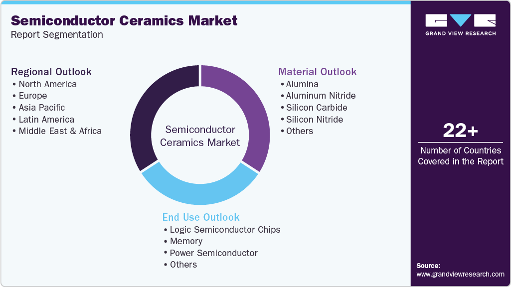
This report forecasts revenue and volume growth at global, regional, and country levels and provides an analysis of the latest industry trends in each of the sub-segments from 2021 to 2033. For the purpose of this study, Grand View Research has segmented the global semiconductor ceramics market report on the basis of end use, material, and region.
-
End Use Outlook (Revenue, USD Million, 2021 - 2033)
-
Logic Semiconductor Chips
-
Memory
-
Power Semiconductor
-
Others
-
-
Material Outlook (Revenue, USD Million, 2021 - 2033)
-
Alumina
-
Aluminum Nitride
-
Silicon Carbide
-
Silicon Nitride
-
Others
-
-
Regional Outlook (Revenue, USD Million, 2021 - 2033)
-
North America
-
U.S.
-
Canada
-
Mexico
-
-
Europe
-
Germany
-
Ireland
-
France
-
Netherlands
-
-
Asia Pacific
-
China
-
South Korea
-
Japan
-
Taiwan
-
-
Latin America
-
Brazil
-
-
Middle East & Africa
-
Research Methodology
The semiconductor ceramics market figures in this report are based on a proven research process that combines executive interviews with secondary research from proprietary databases, company filings, and recognized regulatory and institutional sources. Market size is built through value-chain sizing-reconciling supply-side and demand-side estimates-and triangulated with bottom-up and top-down approaches. Every estimate passes multiple levels of expert validation before publication, with each semiconductor ceramics segment quantified using the revenue-capture definitions in the table below.
Segment Definition
End Use
Revenue Capture Definition
Logic Semiconductor Chips
Revenue is generated from semiconductor ceramic components used in logic chip manufacturing, including advanced processors, CPUs, GPUs, AI accelerators, and ASICs. Demand is driven by high-performance computing, artificial intelligence, cloud infrastructure, and advanced semiconductor process nodes requiring high-purity, plasma-resistant ceramic components.
Memory
Revenue is derived from semiconductor ceramics used in the production of DRAM, NAND Flash, HBM, and other memory devices. Ceramic components are widely utilized in wafer processing, deposition, etching, and packaging equipment to ensure contamination-free manufacturing and high production yields.
Power Semiconductor
Revenue is generated from ceramic materials and components used in the manufacturing of power semiconductor devices, including SiC and GaN power electronics, IGBTs, MOSFETs, and power modules. Growth is supported by increasing demand from electric vehicles, renewable energy systems, industrial automation, and power infrastructure.
Others
Includes revenue from semiconductor ceramics used in analog, RF, MEMS, optoelectronic, sensor, photonic, and discrete semiconductor manufacturing, as well as research laboratories and specialty semiconductor applications.
Material
Revenue Capture Definition
Alumina
Revenue is generated from alumina-based ceramic components used in electrostatic chucks, chamber liners, insulators, wafer carriers, and semiconductor process equipment due to their excellent electrical insulation, wear resistance, and cost-effectiveness.
Aluminum Nitride
Revenue is derived from aluminum nitride ceramics used in semiconductor substrates, ceramic heaters, and thermal management components, where high thermal conductivity and electrical insulation are essential for advanced semiconductor manufacturing.
Silicon Carbide
Revenue is generated from silicon carbide ceramic components used in plasma-facing semiconductor equipment, susceptors, focus rings, and wafer processing systems due to their exceptional plasma resistance, thermal stability, and mechanical strength.
Silicon Nitride
Revenue is captured from silicon nitride ceramic components utilized in high-strength precision parts, wafer handling systems, bearings, and semiconductor processing equipment requiring superior fracture toughness and wear resistance.
Others
Includes revenue from quartz, yttria, zirconia, boron nitride, and other advanced ceramic materials used in specialized semiconductor manufacturing applications such as plasma etching, CVD/PVD processes, ion implantation, and advanced semiconductor packaging.
Estimation Model
Layer Name
Key Question
Description
Semiconductor Manufacturing Demand Base Layer
What forms the demand base?
Identify global demand from major semiconductor manufacturing industries, including foundries, integrated device manufacturers (IDMs), OSAT companies, and semiconductor equipment manufacturers. Assess semiconductor wafer production, fab expansions, equipment installations, and investments in AI, memory, logic, power, and analog semiconductor manufacturing to establish the total addressable demand for semiconductor ceramics.
Semiconductor Ceramics Application Penetration Layer
Where are semiconductor ceramics utilized?
Estimate the penetration of semiconductor ceramics across key applications, including electrostatic chucks, chamber liners, focus rings, ceramic heaters, wafer carriers, gas distribution plates, insulators, and semiconductor packaging substrates. Analyze the adoption of alumina, aluminum nitride, silicon carbide, silicon nitride, quartz, yttria, and zirconia across semiconductor fabrication, wafer processing, and advanced packaging applications by region.
Semiconductor Ceramics Consumption Intensity Layer
How much semiconductor ceramics are consumed?
Analyze semiconductor ceramics consumption intensity based on semiconductor fabrication capacity, wafer starts, equipment installations, and advanced packaging production. Evaluate ceramic component usage per semiconductor processing tool according to process node, wafer size, plasma exposure, thermal management requirements, and replacement cycles. Consumption intensity varies depending on equipment type, manufacturing technology, ceramic material, and semiconductor production volume.
Revenue Layer
How is market revenue generated?
Market revenue is generated through the sale of advanced ceramic materials and precision-engineered ceramic components used in semiconductor manufacturing equipment and electronic packaging. Revenue growth is driven by increasing semiconductor fabrication investments, demand for advanced process equipment, adoption of AI and high-performance computing chips, technological advancements in semiconductor manufacturing, and the use of high-purity ceramic materials for contamination-free wafer processing.
Delivered Customizations
This report has been delivered with the following In-depth customizations
Client Request
Customization Delivered
Value Adds
Regional Segmentation
Detailed regional and country-level analysis across North America, Europe, Asia Pacific, Latin America, and the Middle East & Africa. Included semiconductor fabrication capacity, wafer production, semiconductor equipment manufacturing, government incentives, end-use industry demand, and regional supply chain assessment.
Identified high-growth semiconductor manufacturing hubs and investment hotspots. Supported regional expansion planning, production localization, and market entry strategies.
Pricing Analysis
Comprehensive analysis of semiconductor ceramic pricing by material type, component type, manufacturing process, and region. The study includes historical and forecast price trends, raw material cost movements, energy and processing costs, supply-demand dynamics, and the impact of semiconductor capital expenditure cycles on pricing.
Improved procurement planning and pricing strategy by identifying key cost drivers, regional price variations, and future pricing trends. Supported contract negotiations, supplier evaluation, cost optimization, and profitability analysis.
Trade & Manufacturing Capacity Assessment
In-depth assessment of global manufacturing capacities, production footprints, import-export volumes, trade flows, and country-wise dependence on semiconductor ceramic imports and exports. The analysis includes major manufacturing hubs, capacity expansion projects, raw material availability, supply chain mapping, logistics routes, and regional production versus consumption trends.
Identified supply-demand gaps, manufacturing expansion opportunities, trade risks, and import dependency across key markets. Enabled sourcing diversification, capacity planning, supply chain optimization, and strategic decisions for regional manufacturing and international market expansion.
Frequently Asked Questions About This Report
The global semiconductor ceramics market size was estimated at USD 10.0 billion in 2025 and is expected to reach USD 10.7 billion in 2026.
The global semiconductor ceramics market is expected to grow at a compound annual growth rate of 6.5% from 2026 to 2033 to reach USD 16.7 billion by 2033.
By end use, logic semiconductor chips accounted for the largest market revenue share of 41.4% in 2025.
Asia Pacific dominated the semiconductor ceramics market with the largest revenue share of 73.9% in 2025.
The key factor driving the growth of the global semiconductor ceramics market is the rapid expansion of semiconductor fabrication capacity fueled by increasing demand for AI, 5G, high-performance computing, automotive electronics, and advanced semiconductor manufacturing technologies.
Some of the key players of the global semiconductor ceramics market are CeramTec GmbH, CoorsTek, Inc., Ferrotec Holdings Corporation, Kyocera Corporation, MARUWA Co., Ltd., Morgan Advanced Materials plc, NGK Insulators, Ltd., Ortech Advanced Ceramics, Saint-Gobain Ceramics, Schunk Xycarb Technology, and others.
The semiconductor ceramics market in China held the largest share in the Asia Pacific region in 2025.
By material, the aluminum nitride segment is anticipated to register the fastest CAGR of 6.9% from 2026 to 2033.
The logic semiconductor chips segment is expected to register the highest growth rate during the forecast period, driven by increasing demand for AI, high-performance computing, 5G, and advanced semiconductor devices.
About the Author(s)
Advanced Interior Materials Research Team
Advanced Materials · Advanced Interior MaterialsThis report was authored by the advanced interior materials research team at Grand View Research - comprising two research analysts, one senior research analyst, and one industry expert - with specialized expertise in the advanced interior materials segment of the advanced materials industry. All findings are based on proprietary advanced materials databases, executive interviews, and regulatory analysis, subject to internal peer review prior to publication.
Last Updated:
Speak to Analyst


Customize this report to your needs — add regions, segments, or data points, with 20% free customization.
Or view our licence options:


ISO 9001:2015 & 27001:2022 Certified
We are GDPR and CCPA compliant! Your transaction & personal information is safe and secure. For more details, please read our privacy policy.