
- Home
- »
- Advanced Interior Materials
- »
-
Semiconductor Wafer Polishing And Grinding Equipment Market Report, 2033GVR Report cover

Semiconductor Wafer Polishing And Grinding Equipment Market (2026 - 2033)
Size, Share & Trends Analysis Report By Product (Polishing Machine, Grinding Machine), By Wafer Size, By End Use, By Region, And Segment Forecasts
Market Size, 2025
$2.9BMarket Estimate, 2026
$3.0BMarket Forecast, 2033
$4.3BCAGR, 2026–2033
4.9%Semiconductor Wafer Polishing And Grinding Equipment Market Summary
The global semiconductor wafer polishing and grinding equipment market size was valued at USD 2.9 billion in 2025 and is projected to grow from USD 3.0 billion in 2026 to USD 4.3 billion by 2033, at a CAGR of 4.9% from 2026 to 2033. Asia Pacific dominated the market, accounting for a revenue share of 68.0% in 2025. The global market is experiencing robust growth, propelled by the surging demand for consumer electronics such as smartphones, tablets, and wearables.
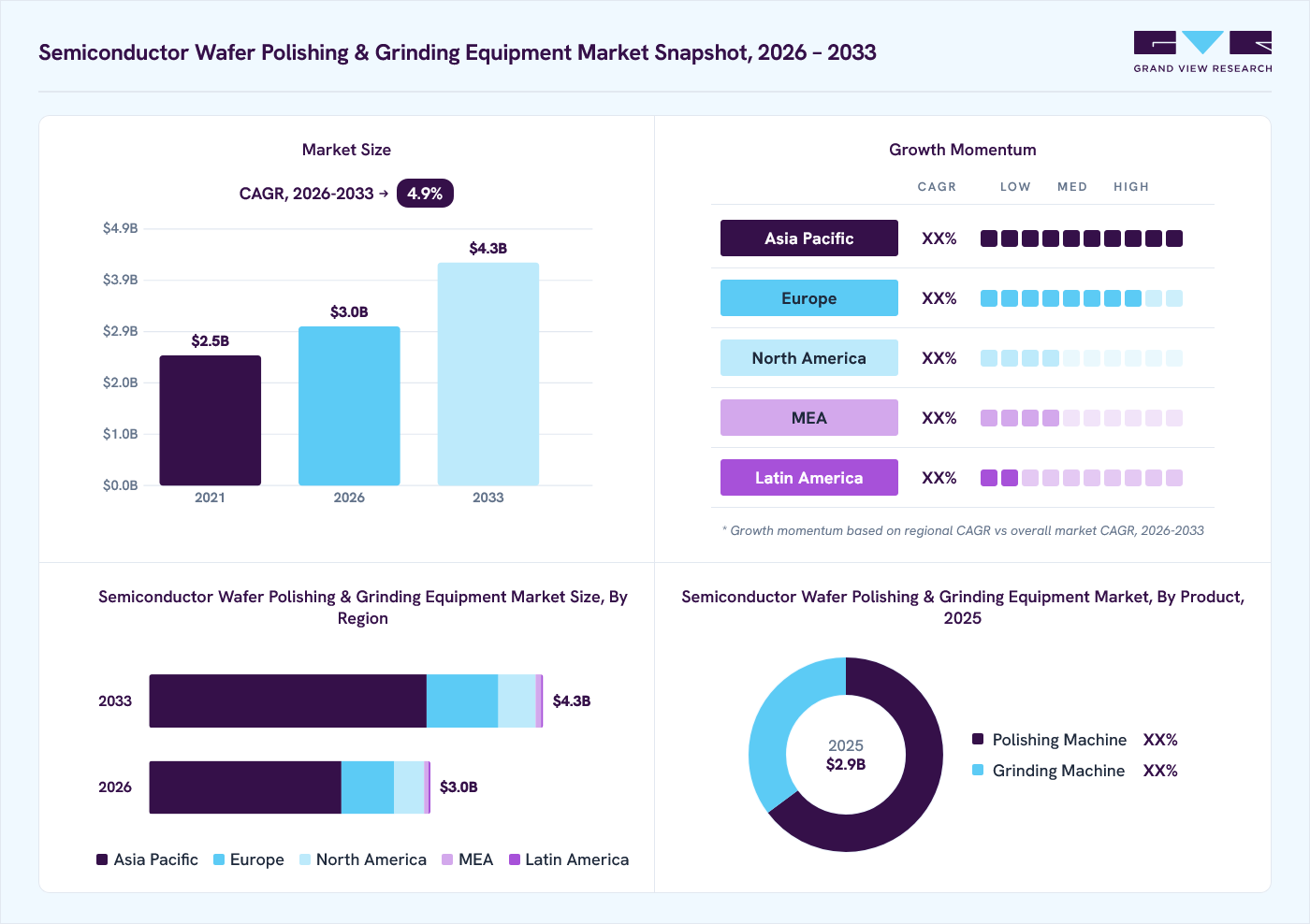 Source: Grand View Research, IR Documents, Primary Interviews, Paid DatabasesTo learn more about this report,
 Download Free Sample Report
Key Market Trends & Insights
- By product: Polishing machine segment led the market with the largest revenue share of 64.8% in 2025.
- By wafer size: 300mm segment led the market with the largest revenue share of 61.9% in 2025.
- By end use: Foundries segment led the market with the largest revenue share of 55.1% in 2025.
Regional Highlights
- Largest regional market: Asia Pacific (68.0% revenue share, 2025)
- By country: The Taiwan held the largest market share in 2025.
Market Size & Forecast
- Market size in 2025: USD 2.9 Billion
- Estimated market size in 2026: USD 3.0 Billion
- Projected market size by 2033: USD 4.3 Billion
- CAGR (2026-2033): 4.9%
Prism AI by Grand View Research Free to tryAsk a question about the semiconductor wafer polishing and grinding equipment marketTry asking✓Every figure cited from GVR research Prefer the report? Download free sample →
The global semiconductor wafer polishing and grinding equipment market size was valued at USD 2.8 billion in 2024 and is projected to grow from USD 3 billion in 2026 to USD 3.7 billion by 2030, at a CAGR of 4.7% from 2025 to 2030. Asia Pacific dominated the market, accounting for a revenue share of 68.7% in 2024. The global market is experiencing robust growth, propelled by the surging demand for consumer electronics such as smartphones, tablets, and wearables. As these devices require increasingly advanced integrated circuits, the need for highly precise wafer polishing and grinding processes has become essential. This trend underscores the critical role of precision manufacturing in enhancing semiconductor performance, efficiency, and miniaturization.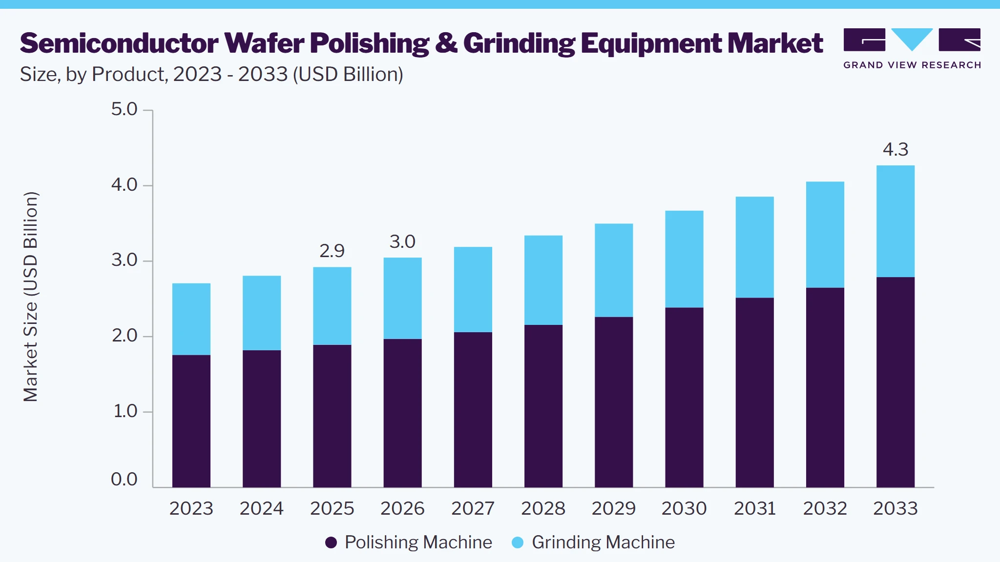 To learn more about this report, Download Free Sample Report
The rapid advancement of technologies like 5G, artificial intelligence (AI), and the Internet of Things (IoT) is driving the need for more sophisticated semiconductor components, further boosting demand for wafer polishing and grinding equipment. The growing adoption of autonomous vehicles, high-performance computing, and advanced data centers is also fueling the need for ultra-precise and high-quality semiconductor wafers.
Market Dynamics
The global semiconductor wafer polishing and grinding equipment market is driven by the rapid expansion of semiconductor manufacturing to support growing demand from artificial intelligence (AI), high-performance computing, 5G networks, automotive electronics, data centers, and advanced consumer devices. Increasing investments in new wafer fabrication facilities, capacity expansions, and advanced process technologies are fueling the need for highly precise polishing and grinding solutions that ensure superior wafer quality, dimensional accuracy, and production efficiency. The market is also benefiting from rising adoption of silicon carbide (SiC) and gallium nitride (GaN) semiconductors used in electric vehicles, renewable energy systems, and industrial power applications, which require specialized wafer processing capabilities. Advancements in chemical mechanical polishing (CMP), automation, metrology integration, and process control technologies are further improving throughput and yield performance. However, high equipment acquisition costs, complex manufacturing requirements, and cyclical fluctuations in semiconductor capital expenditures continue to pose challenges. At the same time, government initiatives to strengthen domestic semiconductor production, ongoing fab construction projects, and increasing adoption of advanced packaging and heterogeneous integration technologies are creating new growth opportunities for equipment providers across global markets.
The increasing deployment of semiconductors in artificial intelligence (AI), high-performance computing, 5G infrastructure, automotive electronics, and cloud computing applications is driving the need for higher wafer production volumes and tighter manufacturing specifications. As chipmakers pursue greater performance, energy efficiency, and device miniaturization, demand for precision polishing and grinding equipment is rising to support critical wafer preparation processes and improve manufacturing outcomes.
Simultaneously, substantial investments in new fabrication facilities and capacity expansion projects across key semiconductor-producing regions are strengthening equipment demand. National semiconductor development programs, supply chain diversification efforts, and strategic investments in domestic chip manufacturing are further accelerating the adoption of advanced wafer processing technologies, supporting long-term market growth.
The adoption of semiconductor wafer polishing and grinding equipment is constrained by significant capital requirements associated with acquiring, installing, and maintaining highly sophisticated processing systems. The need for continuous technology upgrades to meet evolving production standards further increases operational expenditures, particularly for manufacturers operating under tight budget constraints.
Additionally, the transition toward advanced semiconductor nodes and increasingly complex device structures places greater demands on wafer processing accuracy and consistency. Maintaining stringent quality standards while minimizing material loss and process variability requires specialized expertise and sophisticated process management, creating operational challenges that can limit market expansion.
The growing commercialization of silicon carbide (SiC) and gallium nitride (GaN) semiconductors presents a significant opportunity for equipment manufacturers. These materials are gaining traction in electric vehicles, renewable energy systems, and industrial power electronics due to their superior performance characteristics, creating demand for specialized grinding and polishing solutions capable of handling advanced substrate materials.
Furthermore, the increasing adoption of advanced packaging technologies, including chiplet-based designs, 3D integration, and heterogeneous packaging, is generating new requirements for wafer thinning and surface finishing processes. As semiconductor manufacturers focus on maximizing performance within compact form factors, demand for next-generation wafer processing equipment is expected to grow, creating opportunities for innovation and market differentiation.
Market Concentration & Characteristics
The global semiconductor wafer polishing and grinding equipment industry is moderately concentrated, with a mix of large multinational companies and specialized regional players vying for market share. Leading manufacturers in this market are focused on offering cutting-edge equipment that delivers high precision, improved efficiency, and superior surface quality for semiconductor wafer processing. These players are investing heavily in research and development to introduce innovative solutions that cater to the needs of advanced semiconductor manufacturing, including the latest technologies for miniaturization, higher yields, and greater wafer throughput.
Regulatory standards, such as those from the International Electrotechnical Commission (IEC) and other governing bodies, play a crucial role in shaping the competitive landscape of the wafer polishing and grinding equipment industry. Manufacturers must ensure compliance with these stringent requirements, which govern product safety, performance, and environmental standards. With increasing emphasis on sustainability, companies are also looking for ways to reduce energy consumption and waste during the wafer processing stages, aligning with broader industry efforts to minimize the environmental impact of semiconductor manufacturing.
 To learn more about this report, Download Free Sample Report
As demand for high-performance semiconductors rises, driven by industries like artificial intelligence, automotive, and consumer electronics, manufacturers are adapting to the rapid pace of innovation. The integration of advanced automation, smart technologies, and artificial intelligence within semiconductor fabrication plants is creating opportunities for synergies with equipment suppliers. However, the market faces competition from alternative technologies and innovative fabrication methods that could challenge traditional polishing and grinding equipment. To stay competitive, companies must continually innovate, comply with evolving regulations, and meet the growing demand for energy-efficient and high-quality semiconductor production equipment.
Analyst Perspective
The global semiconductor wafer polishing and grinding equipment market is expected to grow steadily, driven by increasing semiconductor production and evolving fabrication requirements. Demand for advanced wafer processing solutions is rising as manufacturers seek higher levels of surface quality, dimensional precision, and process consistency. Growing investments in fabrication facility expansion and technology upgrades are supporting equipment adoption across major semiconductor-producing regions. The market is also benefiting from increased utilization of silicon carbide (SiC) and gallium nitride (GaN) substrates in power and high-performance applications. Advanced packaging and heterogeneous integration trends are creating additional demand for wafer thinning and finishing technologies. Although high equipment costs and cyclical capital spending remain industry challenges, continuous innovation is enhancing operational efficiency and manufacturing capabilities. Supply chain localization initiatives are further encouraging investments in semiconductor infrastructure. As a result, the market outlook remains positive, supported by long-term growth across AI, automotive, communications, and industrial electronics applications.
Product Insights
Based on product, the polishing machine segment led the market with the largest revenue share of 64.8% in 2025, driven by the increasing demand for precision in semiconductor manufacturing. As semiconductor devices become smaller and more complex, the need for advanced polishing techniques to achieve the desired surface quality and flatness is crucial for improving device performance.
The grinding machine segment is significantly driven by the increasing demand for efficient thinning and surface preparation of wafers before further processing. The rising complexity of semiconductor manufacturing processes, including the need for fine material removal, is propelling the demand for high-precision grinding machines.
Wafer Size Insights
Based on wafer size, the 300mm segment led the market with the largest revenue share of 61.9% in 2025. The segment is expanding as the size allows for the production of larger quantities of semiconductors per wafer, improving cost efficiency and yield. The shift toward 300 mm wafers in semiconductor manufacturing is driven by the industry's push for higher production volumes to meet global demand.
The 200 mm wafer size segment is still relevant, especially in older semiconductor manufacturing processes, where certain specialized devices are produced. Smaller wafer sizes remain important for specific applications that do not require the high volume capabilities of 300 mm wafers.
End Use Insights
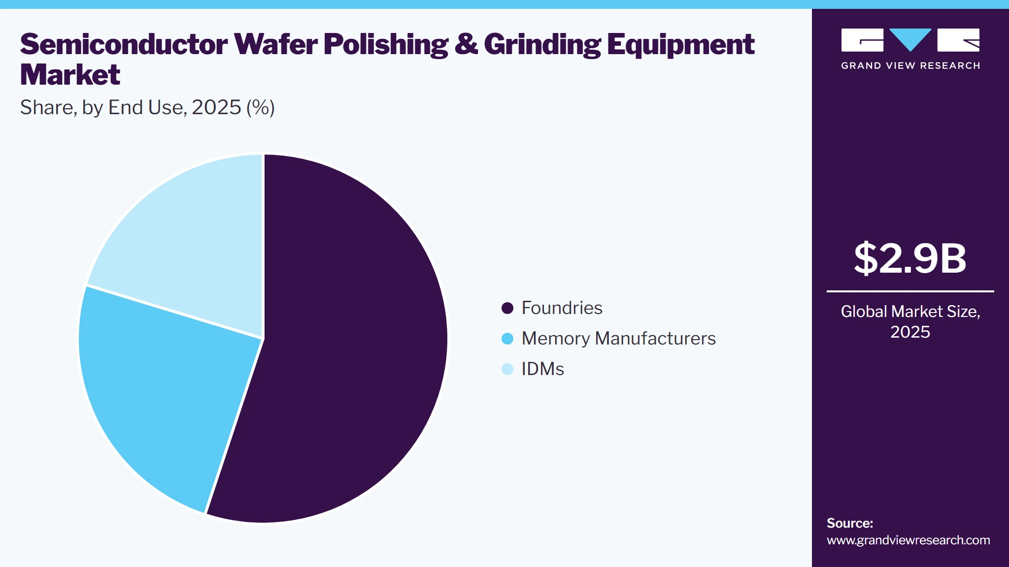
Based on end use, the foundries segment led the market with the largest revenue share of 55.1% in 2025. Foundries are a key driver of market growth, as they serve as the backbone of semiconductor production. With increasing outsourcing of chip manufacturing, foundries are investing in advanced wafer polishing and grinding technologies to meet the high precision and quality requirements of their clients.
 To learn more about this report, Download Free Sample Report
Memory manufacturers are contributing to the market’s growth due to the demand for higher memory capacity and faster processing speeds in consumer electronics. These manufacturers require high-quality wafers that are produced using advanced polishing and grinding techniques to ensure optimal performance in memory chips.
Regional Insights
The semiconductor wafer polishing and grinding equipment market in North America is anticipated to grow at the fastest CAGR during the forecast period. The market is driven by the increasing demand for advanced semiconductors in sectors like automotive, AI, and consumer electronics. The region’s strong technological infrastructure and significant investments in semiconductor manufacturing are also key factors.
U.S. Semiconductor Wafer Polishing And Grinding Equipment Market Trends
The semiconductor wafer polishing and grinding equipment market in the U.S. is projected to grow at the fastest CAGR of 2.8% over the forecast period. In the U.S., market growth is driven by strong demand for advanced semiconductors in sectors like AI, automotive, and consumer electronics, along with significant R&D investments in semiconductor manufacturing.
Asia Pacific Semiconductor Wafer Polishing And Grinding Equipment Market Trends
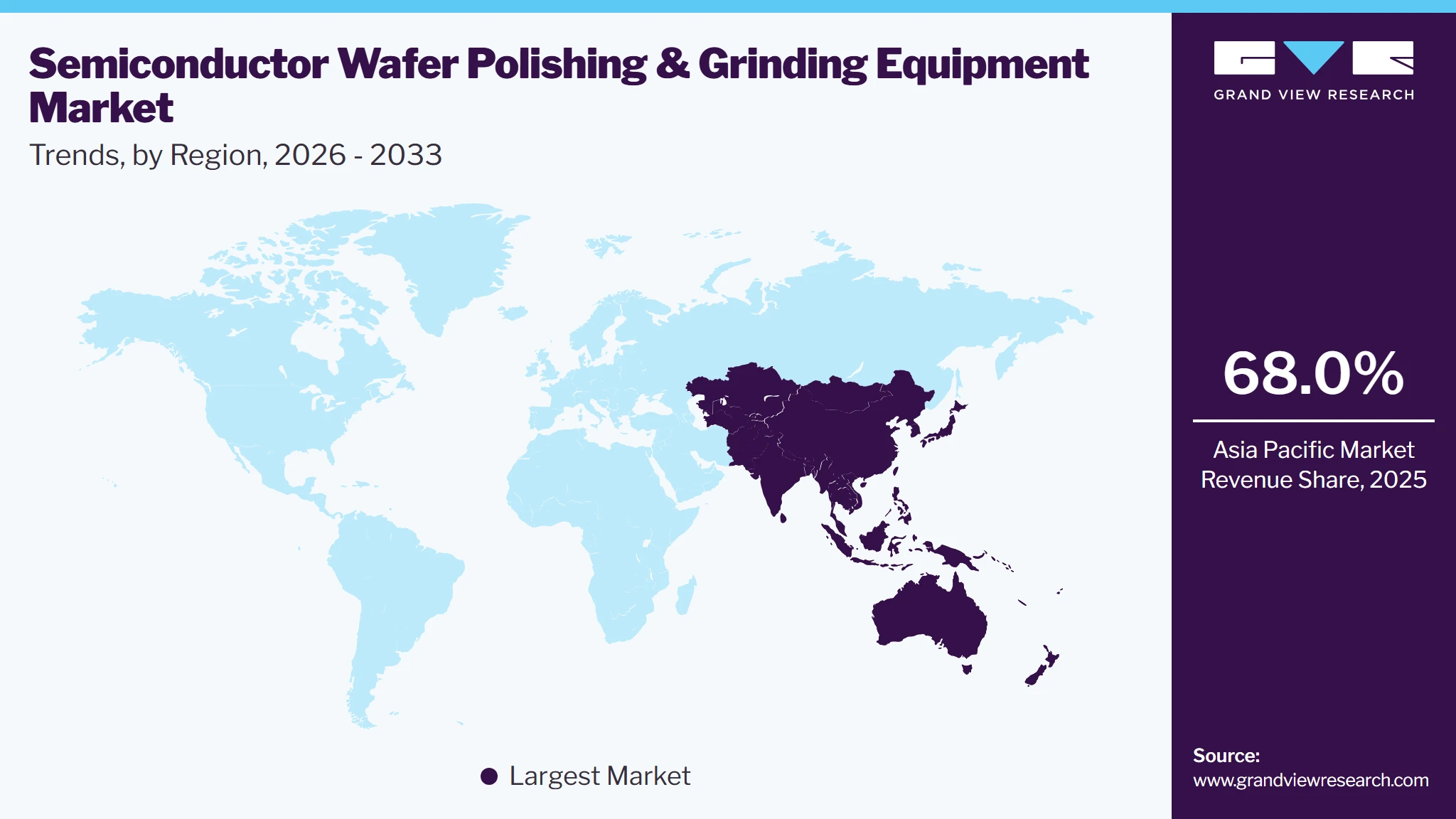
Asia Pacific dominated the global semiconductor wafer polishing and grinding equipment market with the largest revenue share of 68.0% in 2025. The industry in the region benefits from high semiconductor production volumes, especially in countries like China, Japan, South Korea, and Taiwan. The presence of leading semiconductor manufacturers and robust demand for consumer electronics and IoT devices are major growth drivers.
 To learn more about this report, Download Free Sample Report
Taiwan held the largest share in the Asia Pacific region in 2025.
The semiconductor wafer polishing and grinding equipment market in China is projected to grow at a significant CAGR of 6.3% over the forecast period. In China, the semiconductor market is growing rapidly due to its massive electronics production base, government investments in tech infrastructure, and rising demand for consumer electronics and 5G technologies.
The India semiconductor wafer polishing and grinding equipment market is expected to grow at a substantial CAGR of 5.8% over the forecast period, fueled by the country’s expanding electronics manufacturing sector, government initiatives to promote domestic semiconductor production, and a growing consumer electronics market.
Europe Semiconductor Wafer Polishing And Grinding Equipment Market Trends
The semiconductor wafer polishing and grinding equipment market in Europe growth is fueled by the push toward industrial automation, the rise of electric vehicles, and increasing government support for semiconductor innovation and manufacturing within the region.
The Germany semiconductor wafer polishing and grinding equipment market is projected to expand at a significant CAGR of 4.9% over the forecast period. In Germany, the growth is supported by robust industrial automation, the automotive industry's shift to electric vehicles, and government-backed initiatives to boost semiconductor production and technology innovation.
The semiconductor wafer polishing and grinding equipment market in UK is projected to expand at a significant CAGR of 4.4% over the forecast period, driven by increasing demand for high-performance semiconductors, particularly in AI and IoT, along with efforts to bolster the domestic semiconductor manufacturing industry
Middle East & Africa Semiconductor Wafer Polishing And Grinding Equipment Market Trends
The semiconductor wafer polishing and grinding equipment market in the Middle East and Africa is growing due to increased investments in technology and infrastructure, coupled with an expanding electronics sector driven by government-led diversification efforts and the adoption of advanced technologies like AI and renewable energy.
The Saudi Arabiasemiconductor wafer polishing and grinding equipment market is expected to grow at the fastest CAGR of 4.8% over the forecast period, driven by government diversification plans, expanding tech infrastructure, and growing demand for high-tech electronics driven by the Vision 2030 initiative, focusing on innovation and sustainability.
Latin America Semiconductor Wafer Polishing And Grinding Equipment Market Trends
The semiconductor wafer polishing and grinding equipment market in Latin America is driven by emerging manufacturing capabilities, increased demand for consumer electronics, and growing investments in technology infrastructure. As the region develops its semiconductor capabilities, demand for wafer polishing and grinding equipment is expected to rise.
The Argentina semiconductor wafer polishing and grinding equipment market is projected to expand at a significant CAGR of 2.3% over the forecast period. Industry growth in Argentina is driven by increasing investments in technology infrastructure, a rising demand for consumer electronics, and efforts to expand the local manufacturing of electronic components.
Key Semiconductor Wafer Polishing And Grinding Equipment Company Insights
Some of the key players operating in the market include Engis Corporation and Komatsu NTC among others.
-
Engis Corporation is a privately-owned U.S. manufacturer specializing in high-performance superabrasive lapping, grinding, honing, and polishing products, as well as related machinery and accessories. Headquartered in Wheeling, Illinois, the company operates worldwide through subsidiaries in multiple countries and a network of distributors.
-
Komatsu NTC. is a Japanese manufacturer based in Nanto City, Toyama. The company specializes in designing, manufacturing, and selling transfer machines, exclusive-purpose machines, grinding machines, machining centers, crankshaft millers, semiconductor manufacturing equipment, image processing devices, and other related equipment. With a capital of 6,014.55 million yen, the company continues to be a key player in its industry, serving diverse sectors with advanced technological solutions.
Key Semiconductor Wafer Polishing And Grinding Equipment Companies:
The following key companies have been profiled for this study on the semiconductor wafer polishing and grinding equipment market.
-
Engis Corporation
-
Lapmaster Wolters
-
ATM Qness GmbH
-
TOKYO SEIMITSU CO., LTD
-
JOEN LIH MACHINERY CO., LTD
-
SHIN NIPPON KOKI CO., LTD.
-
Qingdao Gaoce Technology Co., Ltd
-
Applied Materials, Inc.
-
DISCO Corporation
-
Fujikoshi Machinery Corp.
-
Komatsu NTC
-
Hapoin Enterprise
-
EBARA Corporation
Competitive Benchmarking
Category
Operating Strategies
Competitive Edge
Weakness
Established Players (e.g., Engis Corporation, Lapmaster Wolters, ATM Qness GmbH, Tokyo Seimitsu Co., Ltd., Applied Materials, Inc., DISCO Corporation, EBARA Corporation, Komatsu NTC)
- Invest heavily in precision processing technologies, automation, and next-generation wafer manufacturing solutions.
- Strengthen market position through long-term partnerships with semiconductor manufacturers and foundries.
- Expand global presence through service networks, product innovation, and advanced equipment portfolios.
- Strong brand reputation and extensive experience in semiconductor manufacturing equipment.
- Broad product portfolios supported by advanced engineering capabilities and global customer support.
- Ability to serve leading-edge semiconductor fabs requiring high precision, reliability, and throughput.
- Premium-priced equipment can limit adoption among cost-sensitive customers.
- Large organizational structures may reduce operational flexibility and responsiveness.
- High dependence on semiconductor capital expenditure cycles can impact revenue growth during industry downturns.
Emerging & Regional Players (e.g., JOEN LIH MACHINERY CO., LTD., Qingdao Gaoce Technology Co., Ltd., Fujikoshi Machinery Corp., Hapoin Enterprise, SHIN NIPPON KOKI CO., LTD., Revasum)
- Focus on specialized applications and cost-competitive wafer processing equipment offerings.
- Emphasize customization and flexibility to address specific customer requirements.
- Target regional semiconductor manufacturing hubs and emerging fabrication markets for growth.
- Competitive pricing strategies help attract budget-conscious customers and regional manufacturers.
- Greater agility in delivering customized solutions and responding to evolving customer needs.
- Strong expertise in selected niche applications and specialized wafer processing requirements.
- Limited global reach and smaller aftermarket service infrastructure compared to industry leaders.
- Lower research and development resources may slow technology advancement.
- Reduced participation in large-scale, leading-edge semiconductor fabrication projects due to narrower capabilities and customer networks.
Recent Developments
-
In February 2022, global semiconductor technology and equipment company, Revasum, Inc. announced it secured a growth capital facility from SQN Venture Partners, LLC, providing up to USD 8 million in debt financing. The funding, split into two tranches, will accelerate new product development and support working capital for rapid growth.
-
In December 2024, Tokyo Electron Limited launched the Ulucus LX, a system using Extreme Laser Lift Off technology for 300mm wafer-bonded devices. This system addresses the growing need for improved semiconductor performance and energy efficiency through 3D integration using permanent wafer bonding. The Ulucus LX performs laser beam irradiation, wafer removal, and cleaning in one unit, integrating TEL's laser control, wafer separation expertise, and cleaning technologies. The system aims to replace multiple processes like back grinding, polishing, and chemical etching, improving productivity and reducing environmental impact.
Semiconductor Wafer Polishing And Grinding Equipment Market Report Scope
Report Attribute
Details
Market size in 2025
USD 2.9 billion
Estimated market size in 2026
USD 3.0 billion
Projected market size by 2033
USD 4.3 billion
Growth rate
CAGR of 4.9% from 2026 to 2033
Base year for estimation
2025
Historical data
2021 - 2024
Forecast period
2026 - 2033
Quantitative units
Revenue in USD billion and CAGR from 2026 to 2033
Report coverage
Revenue forecast, company ranking, competitive landscape, growth factors, and trends
Segments covered
Product, wafer size, end use, region
Regional scope
North America; Europe; Asia Pacific; Latin America; Middle East & Africa
Country scope
U.S.; Canada; Mexico; Germany; UK; France; Italy; Spain; Japan; China; India; Taiwan; South Korea; Brazil; Argentina; Saudi Arabia; South Africa; UAE
Key companies profiled
Engis Corporation; Lapmaster Wolters; ATM Qness GmbH; TOKYO SEIMITSU CO., LTD; JOEN LIH MACHINERY CO., LTD; SHIN NIPPON KOKI CO., LTD.; Qingdao Gaoce Technology Co., Ltd; Applied Materials, Inc.; DISCO Corporation; Revasum; Fujikoshi Machinery Corp.; Komatsu NTC; Hapoin Enterprise; and EBARA Corporation.
Customization scope
Free report customization (equivalent up to 8 analysts' working days) with purchase. Addition or alteration to country, regional & segment scope.
Pricing and purchase options
Avail customized purchase options to meet your exact research needs. Explore purchase options
Global Semiconductor Wafer Polishing And Grinding Equipment Market Report Segmentation
This report forecasts revenue growth at global, regional & country levels and provides an analysis of the industry trends in each of the sub-segments from 2021 to 2033. For the purpose of this study, Grand View Research has segmented the global semiconductor wafer polishing and grinding equipment market report based on the product, wafer size, end use, and region:
 To learn more about this report, Download Free Sample Report
-
Product Outlook (Revenue, USD Million, 2021 - 2033)
-
Polishing Machine
-
Single Side Polishing Machine
-
Double Side Polishing Machine
-
-
Grinding Machine
-
-
Product Outlook (Revenue, USD Million, 2021 - 2033)
-
300 mm
-
200 mm
-
Less than 200 mm
-
-
End Use Outlook (Revenue, USD Million, 2021 - 2033)
-
Foundries
-
Memory Manufacturers
-
IDMs
-
-
Regional Outlook (Revenue, USD Million, 2021 - 2033)
-
North America
-
U.S.
-
Canada
-
Mexico
-
-
Europe
-
UK
-
Germany
-
France
-
Italy
-
Spain
-
-
Asia Pacific
-
China
-
India
-
Japan
-
South Korea
-
Taiwan
-
-
Latin America
-
Brazil
-
Argentina
-
-
Middle East & Africa
-
South Africa
-
Saudi Arabia
-
UAE
-
-
Research Methodology
The semiconductor wafer polishing and grinding equipment market figures in this report are based on a proven research process that combines executive interviews with secondary research from proprietary databases, company filings, and recognized regulatory and institutional sources. Market size is built through value-chain sizing - reconciling supply-side and demand-side estimates - and triangulated with bottom-up and top-down approaches. Every estimate passes multiple levels of expert validation before publication, with each semiconductor wafer polishing and grinding equipment segment quantified using the revenue-capture definitions in the table below.
Segment Definition
Segment - Product
Revenue Capture Definition
Polishing Machine
The polishing machine segment captures revenue generated from equipment used to improve wafer surface quality, flatness, and planarity during semiconductor manufacturing.
Grinding Machine
The grinding machine segment includes revenue from equipment used for wafer thinning, thickness control, edge shaping, and surface preparation prior to polishing and device fabrication.
Segment - Wafer Size
Revenue Capture Definition
300 mm
The 300 mm segment captures revenue from polishing and grinding equipment designed for processing 300 mm wafers used in high-volume semiconductor manufacturing.
200 mm
The 200 mm segment includes revenue from equipment utilized in the processing of 200 mm wafers.
Less than 200 mm
This segment encompasses revenue from polishing and grinding equipment designed for wafers smaller than 200 mm.
Segment - End Use
Revenue Capture Definition
Foundries
The foundries segment captures revenue from polishing and grinding equipment supplied to contract semiconductor manufacturers that produce wafers and integrated circuits for external customers.
Memory Manufacturers
The memory manufacturers segment includes revenue from equipment deployed in facilities producing memory semiconductors, including DRAM, NAND flash, and other data storage technologies.
IDMs (Integrated Device Manufacturers)
The IDMs segment captures revenue from polishing and grinding equipment purchased by companies that conduct semiconductor design, fabrication, assembly, and commercialization within integrated operations.
Estimation Model
Layer Name
Key Question
Description
Semiconductor Manufacturing Footprint Layer
Which facilities form the addressable market?
Quantify the global base of semiconductor fabrication facilities, including foundries, memory manufacturers, and integrated device manufacturers (IDMs). Assess production scale, fabrication activity, technology mix, and geographic distribution to establish the total market potential for wafer processing equipment.
Process Criticality Layer
Where are polishing and grinding operations essential?
Evaluate the extent to which wafer polishing and grinding are required across semiconductor manufacturing workflows. Analyze requirements driven by surface finish standards, wafer thickness specifications, material characteristics, and device performance objectives across logic, memory, power, and specialty semiconductor production.
Technology Adoption Layer
What share of eligible facilities utilizes these solutions?
Measure the installed base and penetration of polishing and grinding systems across fabrication environments. Consider equipment preferences by manufacturing segment, wafer material, production sophistication, automation level, and replacement cycles to determine overall technology adoption.
Revenue Conversion Layer
How does installed demand translate into market value?
Convert equipment demand into revenue using pricing benchmarks across polishing and grinding platforms, performance configurations, and service offerings. Revenue generation incorporates new system sales, facility upgrades, refurbishment programs, spare parts, maintenance contracts, and technical support services.
Delivered Customizations
This report has been delivered with the following In-depth customizations
CLIENT REQUEST
CUSTOMIZATION DELIVERED
VALUE ADDS
Competitive Benchmarking
Benchmarked leading semiconductor wafer polishing and grinding equipment manufacturers based on product portfolio breadth, technological expertise, financial performance, customer focus, geographic reach, and strategic positioning, while distinguishing established market leaders from emerging participants.
Delivered a clear view of the competitive environment, enabling the client to evaluate market standing, assess differentiation factors, uncover partnership opportunities, and track competitive developments.
Regional Segmentation
Refined regional analysis by assessing semiconductor fabrication capacity, wafer production trends, policy support initiatives, capital expenditure activity, and manufacturing ecosystem maturity across North America, Europe, Asia Pacific, Latin America, and the Middle East & Africa.
Highlighted priority markets, regional demand patterns, and expansion potential, supporting strategic decision-making related to market entry, resource deployment, and geographic growth initiatives.
Opportunity assessment
Evaluated emerging opportunities across advanced process nodes, compound semiconductor production (SiC and GaN), advanced packaging technologies, wafer size migration trends, and automated wafer processing solutions.
Enabled prioritization of the most attractive revenue pools by identifying technology segments and application areas expected to benefit from sustained industry adoption and capacity expansion.
Frequently Asked Questions About This Report
Some of the key players operating in the Semiconductor Wafer Polishing and Grinding Equipment Market are Engis Corporation, Lapmaster Wolters, ATM Qness GmbH, TOKYO SEIMITSU CO., LTD, JOEN LIH MACHINERY CO., LTD, SHIN NIPPON KOKI CO., LTD., Qingdao Gaoce Technology Co., Ltd, Applied Materials, Inc., DISCO Corporation, Revasum, Fujikoshi Machinery Corp., Komatsu NTC, Hapoin Enterprise, and EBARA Corporation.
The global semiconductor wafer polishing and grinding equipment market size was valued at USD 2.9 billion in 2025 and is estimated at USD 3.0 billion for 2026.
Asia Pacific dominated with a 68.0% revenue share in 2025.
Key factors driving the Semiconductor Wafer Polishing and Grinding Equipment Market include the increasing demand for smaller, high-performance semiconductors and advancements in semiconductor manufacturing technologies, such as 5G, AI, and IoT.
The global semiconductor wafer polishing and grinding equipment market is expected to grow at a CAGR of 4.9% from 2026 to 2033, reaching USD 4.3 billion by 2033.
About the Author(s)
Advanced Interior Materials Research Team
Advanced Materials · Advanced Interior MaterialsThis report was authored by the advanced interior materials research team at Grand View Research - comprising two research analysts, one senior research analyst, and one industry expert - with specialized expertise in the advanced interior materials segment of the advanced materials industry. All findings are based on proprietary advanced materials databases, executive interviews, and regulatory analysis, subject to internal peer review prior to publication.
Last Updated:
Speak to Analyst

Customize this report to your needs - add regions, segments, or data points, with 20% free customization.
Or view our licence options:


ISO 9001:2015 & 27001:2022 Certified
We are GDPR and CCPA compliant! Your transaction & personal information is safe and secure. For more details, please read our privacy policy.


