- Home
- »
- Advanced Interior Materials
- »
-
U.S. Semiconductor Assembly And Packaging Equipment Market 2033GVR Report cover
![U.S. Semiconductor Assembly And Packaging Equipment Market Size, Share & Trends Report]()
U.S. Semiconductor Assembly And Packaging Equipment Market (2025 - 2033) Size, Share & Trends Analysis Report By Product (Dicing Equipment, Bonding Equipment), By Packaging Type (Flip Chip Packaging Equipment), By End-use (IDMs), And Segment Forecasts
- Report ID: GVR-4-68040-676-4
- Number of Report Pages: 100
- Format: PDF
- Historical Range: 2021 - 2024
- Forecast Period: 2025 - 2033
- Industry: Advanced Materials
- Report Summary
- Table of Contents
- Segmentation
- Methodology
- Download FREE Sample
-
Download Sample Report
U.S. Semiconductor Assembly And Packaging Equipment Market Summary
The U.S. semiconductor assembly and packaging equipment market size was estimated at USD 440.7 million in 2024 and is projected to reach USD 772.5 million by 2033, growing at a CAGR of 6.6% from 2025 to 2033. The growing adoption of advanced packaging solutions such as 2.5D/3D ICs, fan-out wafer-level packaging (FOWLP), and system-in-package (SiP) is significantly driving market demand in the U.S.
Key Market Trends & Insights
- By product, the bonding equipment segment accounted for a share of 34.8% in 2024.
- By packaging type, wafer-level packaging equipment dominated the U.S. semiconductor assembly and packaging equipment market with a share of 31.9% in 2024.
- By end use, the Integrated Device Manufacturers (IDMs) segment accounted for a share of 57.3% in 2024.
Market Size & Forecast
- 2024 Market Size: USD 440.7 Million
- 2033 Projected Market Size: USD 772.5 Million
- CAGR (2025-2033): 6.6%
These technologies enhance performance, reduce form factor, and improve power efficiency vital for artificial intelligence (AI), IoT, and 5G applications. Strong federal backing through initiatives like the CHIPS and Science Act is catalyzing domestic semiconductor manufacturing and packaging infrastructure. Substantial funding incentives are encouraging companies to establish or expand advanced packaging facilities in the U.S. This support reduces reliance on overseas providers and enhances supply chain resilience. The push toward localized production is especially critical amid rising geopolitical tensions and global supply disruptions.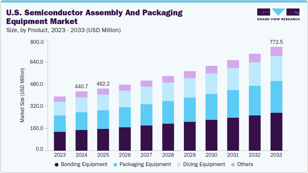
Market Concentration & Characteristics
The U.S. semiconductor assembly and packaging equipment market is moderately concentrated, with a few key players dominating a significant market share. Major companies such as Applied Materials, Intel, and Lam Research lead due to strong technological capabilities and substantial investment in R&D. However, emerging startups and mid-sized firms are gradually entering the space, especially in niche packaging technologies. Despite new entrants, high capital requirements and technical complexity continue to limit widespread competition.
The U.S. semiconductor assembly and packaging equipment industry is highly innovation-driven, with continuous advancements in chip miniaturization and heterogeneous integration. Companies are investing in AI-enabled inspection tools, thermal management solutions, and advanced lithography. Innovation is essential to meet the growing performance and efficiency demands of sectors like automotive, aerospace, and consumer electronics. Frequent technological upgrades help firms maintain competitiveness in a rapidly evolving market.
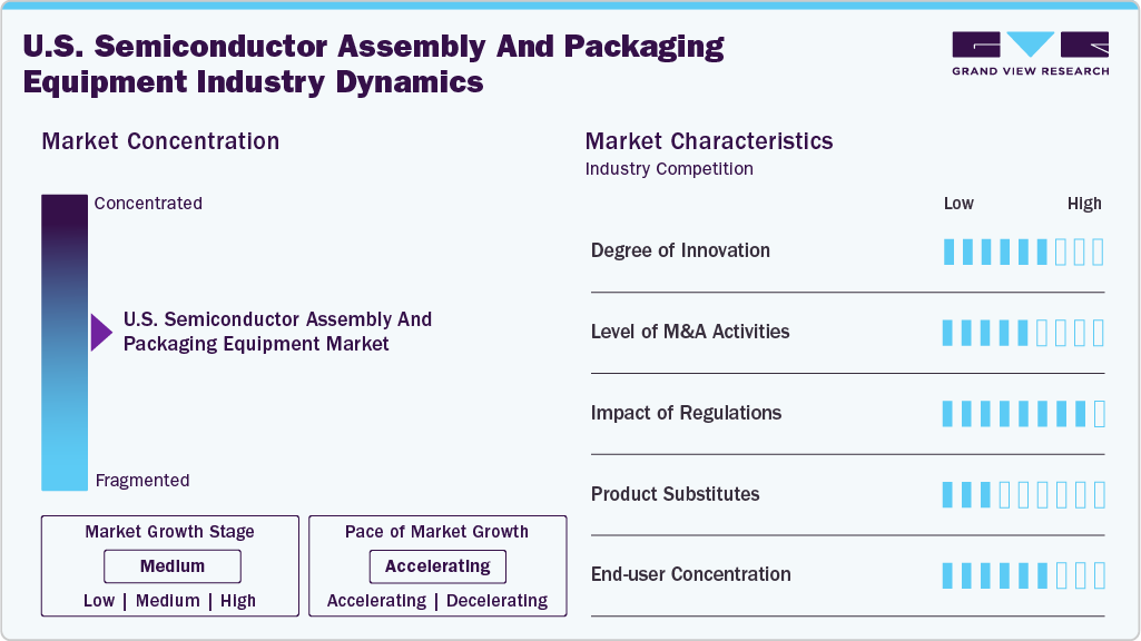
M&A activity in the U.S. market is active, as companies pursue strategic partnerships and acquisitions to expand capabilities and portfolios. Larger players often acquire startups specializing in advanced packaging or automation technologies. This consolidation strengthens market presence and accelerates time-to-market for new solutions. It also allows firms to enhance R&D and better address evolving customer needs.
U.S. government regulations significantly influence the semiconductor equipment market, particularly in areas of export control and domestic manufacturing incentives. Policies such as the CHIPS and Science Act support domestic innovation and infrastructure growth. At the same time, export restrictions on certain technologies to foreign markets impact supply chains and sales strategies. Compliance with safety, environmental, and trade standards remains critical for market players.
Drivers, Opportunities & Restraints
The growing demand for advanced consumer electronics, electric vehicles, and AI-integrated devices is driving the U.S. semiconductor assembly and packaging equipment market. Domestic manufacturing incentives and federal funding are boosting capital investments in packaging infrastructure. The U.S. also benefits from a strong base of tech giants and research institutions fostering innovation. These factors collectively support the rapid adoption of high-performance packaging technologies.
Rising interest in onshore semiconductor production creates opportunities for new facility development and technology integration. The shift toward chiplet architecture and heterogeneous packaging opens doors for specialized equipment providers. Increased government funding and public-private partnerships are fueling collaborative R&D efforts. Additionally, the growing demand for secure and localized supply chains enhances long-term growth potential.
High capital expenditure and long development cycles act as barriers for new entrants in the U.S. market. Skilled labor shortages and talent gaps in advanced packaging technologies pose operational challenges. Geopolitical tensions and trade restrictions may limit access to critical components and international markets. Furthermore, regulatory compliance and environmental standards add complexity and cost to equipment deployment.
Product Insights
The bonding equipment segment accounted for a share of 34.8% in 2024, owing to its critical role in die attach and wire bonding processes. These tools are essential for high-precision packaging in applications such as automotive electronics, high-performance computing, and mobile devices. U.S. manufacturers prioritize bonding technologies that support miniaturization and high-speed data transmission. The ongoing push for 3D and heterogeneous integration further strengthens demand for advanced bonding solutions.
Packaging equipment is experiencing rapid growth in the U.S. semiconductor assembly and packaging equipment industry as demand rises for compact, energy-efficient, and high-performance chips. The surge in AI, IoT, and 5G applications is driving the adoption of innovative packaging formats like SiP and fan-out wafer-level packaging. U.S.-based companies are expanding their capabilities to include automation and thermal management in packaging processes. Government support for domestic semiconductor production is also accelerating investment in advanced packaging infrastructure.
Packaging Type Insights
Wafer-level packaging equipment dominated the U.S. semiconductor assembly and packaging equipment market with a share of 31.9% in 2024, due to its ability to deliver compact, high-performance chips with reduced interconnect lengths and improved thermal efficiency. It is widely used in smartphones, wearables, and automotive electronics, where size and performance are critical. U.S. semiconductor firms favor WLP for its scalability and compatibility with automated production lines. Its integration into advanced node manufacturing further boosts its dominance.

3D/2.5D packaging equipment is the fastest-growing segment, driven by the need for high bandwidth and energy-efficient processing in AI, HPC, and data center applications. These technologies enable chiplet integration and vertical stacking, improving performance while conserving space. U.S. investment in heterogeneous integration and chiplet design is accelerating demand for this equipment. Government-backed initiatives also promote adoption by supporting advanced packaging ecosystems.
End Use Insights
The Integrated Device Manufacturers (IDMs) segment accounted for a share of 57.3% in 2024, due to their end-to-end control over design, fabrication, and packaging. Leading U.S. IDMs like Intel and Texas Instruments invest heavily in advanced packaging technologies to boost performance and reduce costs. Their in-house capabilities allow faster innovation and customization for emerging applications. This vertical integration gives IDMs a competitive edge in quality control and supply chain resilience.
Outsourced Semiconductor Assembly and Test (OSAT) providers are the fastest-growing segment in the U.S. semiconductor assembly and packaging equipment industry, driven by increasing demand for cost-efficient, specialized packaging services. As chip designs grow more complex, fabless companies rely on OSATs for access to advanced packaging technologies. U.S.-based OSATs are expanding their capabilities in areas like fan-out, wafer-level, and 2.5D/3D packaging. Supportive policies and rising demand for flexible supply chains are accelerating this segment’s growth.
Key U.S. Semiconductor Assembly And Packaging Equipment Company Insights
Some of the key players operating in the market include Applied Materials, ASM Pacific Technology, and Veeco Instruments Inc.
-
Applied Materials is a leading supplier of advanced packaging equipment, particularly focused on enabling next-generation chip architectures through technologies like hybrid bonding and wafer-level integration. The company plays a critical role in the evolution of heterogeneous integration and 3D stacking, supporting the performance demands of AI, data centers, and high-performance computing. Its integrated material solutions bridge front-end wafer fabrication and back-end packaging, optimizing interconnect density and power efficiency. Applied Materials also invests heavily in packaging R&D, often collaborating with major IDMs and OSATs to push the limits of system scaling.
-
ASM Pacific Technology focuses heavily on advanced packaging solutions, including fan-out, flip chip, and system-in-package (SiP) technologies tailored for high-density applications. The company delivers precision bonding systems and automation platforms widely adopted by major OSATs and IDMs. It also leads to developing integrated hardware-software solutions to enhance packaging throughput and yield. ASMPT’s innovations directly support miniaturization and heterogeneous integration in next-generation semiconductor devices.
Key U.S. Semiconductor Assembly And Packaging Equipment Companies:
- Applied Materials
- ASM Pacific Technology
- Besi
- Disco Corporation
- Kulicke & Soffa Industries, Inc. (K&S)
- Lam Research Corporation
- Nikon Corporation
- Plasma-Therm
- Rudolph Technologies, Inc.
- SCREEN Semiconductor Solutions Co., Ltd.
Recent Developments
-
In May 2025, Veeco announced receiving over USD 35 million in orders for its AP300 advanced packaging lithography systems from both IDMs and OSATs. These systems will support expanding production needs tied to AI and high-performance computing markets. The AP300 is optimized for applications like copper pillar bumping, flip chip, and fan-out wafer-level packaging. This order boost is expected to strengthen Veeco’s advanced packaging equipment business significantly in 2025.
-
In August 2024, Polymatech, an Indian opto-semiconductor firm, acquired U.S.-based Nisene Technology Group to strengthen its presence in IC packaging and testing. The move supports Polymatech’s goal of building a comprehensive semiconductor ecosystem. It also includes plans for major investments to expand operations in the U.S. This acquisition boosts the company’s capabilities across the chipmaking value chain.
-
In November 2022, Lam Research acquired SEMSYSCO to bolster its advanced packaging capabilities in semiconductor manufacturing. The acquisition enhances its wet processing and panel-level packaging technology for seamless integration in next-generation chip designs. This strategic move is aimed at strengthening its solutions for high-performance computing and AI applications. The deal marks a significant expansion of Lam Research’s portfolio in the advanced packaging ecosystem.
U.S. Semiconductor Assembly And Packaging Equipment Market Report Scope
Report Attribute
Details
Market size value in 2025
USD 462.2 million
Revenue forecast in 2033
USD 772.5 million
Growth rate
CAGR of 6.6% from 2025 to 2033
Historical data
2021 - 2024
Forecast period
2025 - 2033
Quantitative units
Revenue in USD million and CAGR from 2025 to 2033
Report coverage
Revenue forecast, company ranking, competitive landscape, growth factors, and trends
Segments covered
Product, end use, packaging type
Country scope
U.S.
Key companies profiled
Applied Materials; ASM Pacific Technology; Besi; Disco Corporation; Kulicke & Soffa Industries, Inc. (K&S); Lam Research Corporation; Nikon Corporation; Plasma-Therm; Rudolph Technologies, Inc.; SCREEN Semiconductor Solutions Co., Ltd.
Customization scope
Free report customization (equivalent up to 8 analysts working days) with purchase. Addition or alteration to country, regional & segment scope.
Pricing and purchase options
Avail customized purchase options to meet your exact research needs. Explore purchase options
U.S. Semiconductor Assembly And Packaging Equipment Market Report Segmentation
This report forecasts revenue growth at the U.S. level and provides an analysis of the latest industry trends in each of the sub-segments from 2021 to 2033. For this study, Grand View Research has segmented the U.S. semiconductor assembly and packaging equipment market report based on packaging type,end use, and product:
-
Packaging Type Outlook (Revenue, USD Million, 2021 - 2033)
-
Flip Chip Packaging Equipment
-
Wafer Level Packaging (WLP) Equipment
-
Fan-Out Packaging Equipment
-
System-in-Package (SiP) Equipment
-
3D/2.5D Packaging Equipment
-
Others
-
-
End Use Outlook (Revenue, USD Million, 2021 - 2033)
-
IDMs (Integrated Device Manufacturers)
-
OSAT (Outsourced Semiconductor Assembly and Test)
-
-
Product Outlook (Revenue, USD Million, 2021 - 2033)
-
Dicing Equipment
-
Scriber
-
Dicer
-
Wafer Mounting Equipment
-
-
Bonding Equipment
-
Die Bonder
-
Wire Bonder
-
Others
-
-
Packaging Equipment
-
Molding Equipment
-
Solder Plating Equipment
-
Deflasher
-
Others
-
-
Others
-
Frequently Asked Questions About This Report
b. The U.S. semiconductor assembly and packaging equipment market size was estimated at USD 440.7 million in 2024 and is expected to be USD 462.2 million in 2025.
b. The U.S. semiconductor assembly and packaging equipment market, in terms of revenue, is expected to grow at a compound annual growth rate of 6.6% from 2025 to 2033 to reach USD 772.5 million by 2033.
b. Integrated Device Manufacturers (IDMs) segment accounted for a share of 57.3% in 2024, due to their end-to-end control over design, fabrication, and packaging. Leading U.S. IDMs like Intel and Texas Instruments invest heavily in advanced packaging technologies to boost performance and reduce costs. Their in-house capabilities allow faster innovation and customization for emerging applications.
b. Some of the key players operating in the U.S. semiconductor assembly and packaging equipment market include Applied Materials; ASM Pacific Technology; Besi; Disco Corporation; Kulicke & Soffa Industries, Inc. (K&S); Lam Research Corporation; Nikon Corporation; Plasma-Therm; Rudolph Technologies, Inc.; SCREEN Semiconductor.
b. Key factors driving the U.S. semiconductor assembly and packaging equipment market include the rising demand for advanced packaging technologies to support AI, 5G, and high-performance computing. Government initiatives like the CHIPS Act are fueling domestic manufacturing and infrastructure development. Additionally, increased focus on supply chain resilience and localized production is boosting investment in packaging equipment.
Share this report with your colleague or friend.
Need a Tailored Report?
Customize this report to your needs — add regions, segments, or data points, with 20% free customization.

ISO 9001:2015 & 27001:2022 Certified
We are GDPR and CCPA compliant! Your transaction & personal information is safe and secure. For more details, please read our privacy policy.
Trusted market insights - try a free sample
See how our reports are structured and why industry leaders rely on Grand View Research. Get a free sample or ask us to tailor this report to your needs.


