- Home
- »
- Advanced Interior Materials
- »
-
Semiconductor Bonding Market Size & Share Report, 2030GVR Report cover
![Semiconductor Bonding Market Size, Share & Trends Report]()
Semiconductor Bonding Market (2024 - 2030) Size, Share & Trends Analysis Report By Type (Die Bonder, Wafer Bonder, Flip Chip Bonder), By Application (RF Devices, LED, 3D NAND), By Process Type, By Region, And Segment Forecasts
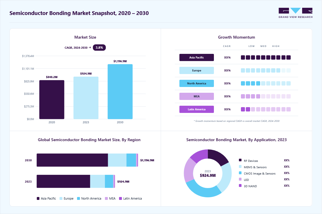
Market Size, 2023
$925.0MMarket Estimate, 2024
$954.5MMarket Forecast, 2030
$1,200.0MCAGR, 2024–2030
3.8%Semiconductor Bonding Market Summary
The global semiconductor bonding market size was estimated at USD 925.00 million in 2023 and is projected to reach USD 1200.0 million by 2030, growing at a CAGR of 3.8% from 2024 to 2030. The market is experiencing robust growth driven by the burgeoning demand for advanced electronic devices such as smartphones, electric vehicles, and renewable energy systems.
Key Market Trends & Insights
- The Asia Pacific region holds a significant share in the global market primarily due to its significant contributions to semiconductor manufacturing.
- The semiconductor bonding market in China is estimated to grow at a significant CAGR of 5.5% over the forecast period.
- Based on process type, the die to die bonding segment led the market and accounted for 51.99% of the global revenue share in 2023.
- Based on type, the die bonder segment accounted for 40.04% of the global market revenue share in 2023.
- Based on application, the CMOS image & sensors application segment accounted for 28.49% of the global market revenue share in 2023.
Market Size & Forecast
- 2023 Market Size: USD 925.00 Million
- 2030 Projected Market Size: USD 1.20 Billion
- CAGR (2024-2030): 3.8%
- Asia Pacific: Largest market in 2023
This market encompasses a wide array of bonding techniques, including die bonding, wafer bonding, and flip-chip bonding, each crucial for producing integrated circuits and microelectronic components. Semiconductor bonding is a critical process in the fabrication of microelectronic devices. It involves joining two semiconductor materials or a semiconductor and another material, such as metal or insulator, to form a functional unit. This process, essential for assembling integrated circuits and forming microelectronic structures, utilizes various techniques such as wafer bonding, die bonding, and flip-chip bonding. The surge in IoT devices and AI applications and the push towards miniaturization and high-performance computing further propel the market.")
Increasing investments in semiconductor manufacturing, the growing need for efficient thermal management, and higher performance in electronic devices are driving the market's expansion. As industries continue to evolve towards more complex and integrated technology solutions, the market is expected to play a key role in shaping the future of global electronics manufacturing.
Market Dynamics
The explosive growth of artificial intelligence (AI) and high-performance computing (HPC) is a primary driver of the semiconductor bonding market. Modern AI workloads and data centers require unprecedented processing speeds and data bandwidth, which traditional 2D chips can no longer sustain. To overcome these physical limitations, the industry is shifting toward chiplet architectures and 3D stacked integrated circuits. These advanced packaging methods rely heavily on sophisticated bonding techniques, such as hybrid bonding and thermocompression bonding, to connect multiple dies with ultra-fine pitch precision, enabling faster data transfer and improved power efficiency.
The production of advanced semiconductor bonding equipment and materials depends on a highly specialized, global network of suppliers. Disruptions in the availability of critical components, ranging from precision optical lenses and robotic components to specialized consumables such as ultra-flat carrier wafers and high-purity adhesives, can lead to severe manufacturing delays. These long lead times prevent equipment manufacturers from meeting sudden surges in market demand, ultimately slowing down the expansion and scaling of advanced packaging facilities worldwide.
Process Type Insights
“The demand for die to wafer bonding segment is expected to grow at a CAGR of 4.5% from 2024 to 2030 in terms of revenue.”
The die to die bonding segment led the market and accounted for 51.99% of the global revenue share in 2023. The die to die (D2D) bonding segment of the market is witnessing significant growth, driven by the increasing complexity and performance requirements of electronic devices. D2D bonding, a critical technique in 3D integration, allows for the vertical stacking of semiconductor chips, leading to considerable enhancements in performance and functionality while reducing space and power consumption. The push towards smaller, faster, and more energy-efficient devices across industries, including consumer electronics and telecommunications, presents substantial opportunities to expand the D2D bonding market.
The Die to Wafer (D2W) bonding market is gaining traction within the semiconductor industry, fueled by the accelerating demand for high-density and high-performance semiconductor devices across various sectors, including consumer electronics, automotive, and healthcare. D2W bonding is crucial for heterogeneous integration, where dies with different functionalities are bonded onto a single wafer, thus enabling the fabrication of complex, multi-functional devices within a compact footprint.
Type Insights
“The demand for wafer bonder segment is expected to grow at a CAGR of 4.3% from 2024 to 2030 in terms of revenue.”
Die bonder segment accounted for 40.04% of the global market revenue share in 2023. The market is driven by the escalating demand for more compact, efficient, and high-performance electronic devices across various applications. Die bonders are pivotal in the assembly process of semiconductors, facilitating the precise placement and attachment of dies onto substrates or into packages. This segment's growth is propelled by advancements in consumer electronics, automotive electronics, and the increasing proliferation of IoT devices requiring sophisticated semiconductor components, which will drive the market.
The market for wafer bonders is witnessing substantial growth, fueled by the ever-increasing demand for advanced semiconductor devices in sectors such as consumer electronics, automotive, healthcare, and telecommunications. Wafer bonders play a crucial role in manufacturing by facilitating the bonding of semiconductor wafers, which is essential for creating multi-layered semiconductor devices. This process is pivotal in producing MEMS (Micro-Electro-Mechanical Systems), 3D integrated circuits, and advanced sensors, integral components of modern electronic devices, from smartphones to autonomous vehicles.
Application Insights
“The demand form LED application segment is expected to grow at a significant CAGR of 4.3 % from 2024 to 2030 in terms of revenue.”
CMOS image & sensors application segment accounted for 28.49% of the global market revenue share in 2023. CMOS images & sensors, pivotal in converting light into electronic signals, are integral to a multitude of applications, from smartphones and digital cameras to automotive safety systems, medical devices, and emerging areas like drones and IoT devices. This wide-ranging applicability propels the demand for advanced semiconductor bonding techniques to enhance these devices' performance, efficiency, and miniaturization. The expansion of smart cities and smart home technologies also contributes to the burgeoning demand for sensors that can capture and process vast amounts of data with high precision and reliability.
")
The market for MEMS and sensors is poised for substantial growth, given their escalating integration into a broad spectrum of applications. This surge is attributed to MEMS and sensors' critical role in enhancing device functionality and intelligence, spanning sectors from automotive and healthcare to consumer electronics and industrial automation. These techniques ensure MEMS and sensor device reliability, performance, and miniaturization.
Regional Insights
The Asia Pacific region holds a significant share in the global market primarily due to its significant contributions to semiconductor manufacturing. This region is home to several key players in the semiconductor industry, including countries like South Korea, Taiwan, China, and Japan, which are leading in semiconductor production and developing cutting-edge semiconductor bonding technologies. The increasing demand for semiconductor devices in the Asia Pacific region, driven by the growth in consumer electronics, automotive, and telecommunications sectors, fuels the market.
“China to witness fastest market growth at 5.5% CAGR”
The semiconductor bonding market in China is estimated to grow at a significant CAGR of 5.5% over the forecast period. China's market is rapidly growing, reflecting the country's ambitious drive to bolster its position in the global semiconductor industry. As one of the largest consumers of semiconductor devices, fuelled by its vast electronics manufacturing sector and booming demand for consumer electronics, China is investing heavily in developing its domestic semiconductor capabilities. This effort is part of a broader strategy to reduce dependence on foreign technology and achieve self-sufficiency in the semiconductor supply chain.
North America Semiconductor Bonding Market Trends
The semiconductor bonding market in North America is significantly fuelled by the growing need for more sophisticated electronic devices across various sectors, such as automotive, consumer electronics, healthcare, and defense. The automotive industry's rapid shift towards electric and autonomous vehicles, which require advanced semiconductor components for better performance and safety features, is a notable example. In addition, the expansion of the IoT, artificial intelligence (AI), and 5G technologies in the region underscores the critical need for reliable and efficient semiconductor bonding solutions to ensure high-performance and miniaturized electronic devices. Hence, it is anticipated to drive the market growth during the projected years.
Europe Semiconductor Bonding Market Trends
The semiconductor bonding market in Europe is predominantly driven by the region's strong focus on innovation, sustainability, and advanced manufacturing technologies. The emphasis on renewable energy sources and energy efficiency is pushing for the adoption of power semiconductors. These components require specialized bonding techniques for optimal performance in converting and managing electrical power. Innovations in 3D ICs (Integrated Circuits), MEMS, and advanced packaging techniques further fuel the European market.
Key Semiconductor Bonding Company Insights
Some of the key players operating in the market include EV Group, ASMPT Semiconductor Solutions, and MRSI Systems (Myronic AB).
-
EV Group (EVG) is a prominent player in the market, renowned for its expertise in wafer bonding and lithography equipment for the microelectronics, compound semiconductor, MEMS, and nanotechnology sectors.The company's product portfolio is diverse, catering to various steps in the semiconductor manufacturing process, including lithography, coating, cleaning, and bonding.
-
ASM Pacific Technology (ASMPT), headquartered in Hong Kong, is a leading supplier in the semiconductor and electronics assembly sectors, offering a comprehensive range of equipment and solutions. The company's extensive portfolio encompasses die-attach, flip chip bonding, encapsulation, and wire bonding, catering to the entire spectrum of assembly processes required for semiconductor device fabrication.
BE Semiconductor Industries NV7, Fasford Technology Co.Ltd (Fuji Group), Kulicke, and Soffa Industries Inc. are some of the emerging market participants.
-
BE Semiconductor Industries NV7's focus on advanced packaging technologies, including die attachment, die sorting, and packaging processes pivotal for producing semiconductor devices. Besi's product offerings are integral to assembling a wide array of devices for applications in consumer electronics, computing, automotive, telecommunications, and other sectors demanding high-quality semiconductor components.
-
Fasford Technology caters to a wide range of applications, including conventional IC assembly and high-density packaging needs from sectors such as consumer electronics, automotive, and industrial electronics.
Key Semiconductor Bonding Companies:
The following are the leading companies in the semiconductor bonding market. These companies collectively hold the largest market share and dictate industry trends.
- EV Group
- ASMPT Semiconductor Solutions
- MRSI Systems. (Myronic AB)
- WestBond Inc
- Panasonic Holding Corporation
- Palomar Technologies
- Dr. Tresky AG7
- BE Semiconductor Industries NV7
- Fasford Technology Co.Ltd (Fuji Group)
- Kulicke and Soffa Industries Inc.
- DIAS Automation (HK) Ltd
- Shibaura Mechatronics Corporation
- SUSS MicroTec SE
- Tokyo Electron Limited
Competitive Benchmarking
Operating Strategies
Competitive Edge
Weaknesses
Mature Players: SUSS MicroTec SE, Besi, EV Group (EVG)
- They invest heavily in advanced packaging technologies, automation capabilities, and precision process integration to support next-generation semiconductor manufacturing requirements.
- Many mature players strengthen their market presence through global service networks, regional manufacturing facilities, and continuous research and development investments.
- Foundational patents in high-speed mechanics, thermal control, and sub-micron optical alignment create immense technical barriers to entry for newcomers.
- Their strong financial capabilities support continuous innovation in advanced bonding technologies.
- Allocating significant engineering and support resources toward maintaining and sourcing components for legacy equipment generations can divert focus from next-generation innovation initiatives.
- Many mature companies remain highly exposed to semiconductor industry cyclicality and fluctuations in capital expenditure.
Emerging Players: HANMI SEOUL, Finetech GmbH & Co. KG
- Emerging players often avoid direct competition with established industry leaders in mainstream semiconductor manufacturing, instead focusing on high-growth niche segments such as Silicon Photonics, Quantum Computing, and MicroLED applications.
- They engineer flexible, multi-process platforms that allow a single machine tool to switch between ultrasonic, thermocompression, and eutectic bonding to appeal to adaptive manufacturing lines.
- They tend to quickly scale their internal knowledge bases by hiring specialized talent from adjacent fields and setting up localized operations in expanding regional markets.
- Unconstrained by legacy infrastructure or long-standing customer requirements, emerging players can develop modern bonding architectures specifically optimized for advanced materials such as Gallium Nitride (GaN) and Silicon Carbide (SiC).
- Streamlined internal structures allow them to advance a tool design from a conceptual prototype to a functioning factory-floor model much faster than highly structured corporate legacy peers.
- Emerging players often lack the large-scale manufacturing footprints and extensive supply chain networks required to rapidly fulfill high-volume equipment orders across multiple global production sites.
- High-end semiconductor equipment R&D requires an intense financial runway; emerging players are highly vulnerable to cash flow pinches if an economic downturn slows customer validation cycles.
Recent Developments
-
In March 2024, TANAKA Kikinzoku Kogyo K.K., a leading company in the precious metals industry, recently pioneered the semiconductor bonding field by developing a gold particle bonding technology. This innovative method utilizes AuRoFUSE, a specialized low-temperature fired paste, to facilitate gold-to-gold bonding in high-density semiconductor mounting applications.
-
In December 2023, Tokyo Electron Kyushu developed an Extreme Laser Lift Off (XLO) technology. This cutting-edge approach is set to revolutionize the field of 3D integration for advanced semiconductor devices that utilize permanent wafer bonding. By enabling precise control and efficient integration processes, XLO technology promises to enhance the performance and reliability of semiconductor devices, paving the way for innovations in the electronics industry.
Semiconductor Bonding Market Report Scope
Report Attribute
Details
Market size value in 2024
USD 954.5 million
Revenue forecast in 2030
USD 1200.0 million
Growth rate
CAGR of 3.8% from 2024 to 2030
Historical data
2018 - 2023
Forecast period
2024 - 2030
Quantitative units
Revenue in USD million/billion and CAGR from 2024 to 2030
Report coverage
Revenue forecast, company market position analysis, competitive landscape, growth factors, and trends
Segments covered
Type, process type, application, region
Regional scope
North America; Europe; Asia Pacific; Latin America; Middle East & Africa
Country Scope
U.S.; Canada; Mexico; Germany; France; Italy; UK; Spain; China; Japan; India; South Korea; Taiwan; Brazil; Argentina; South Africa; Saudi Arabi;, UAE
Key companies profiled
EV Group; ASMPT Semiconductor Solutions; MRSI Systems. (Myronic AB); WestBond Inc.; Panasonic Holding Corporation; Palomar Technologies; Dr. Tresky AG7; BE Semiconductor Industries NV7; Fasford Technology Co.Ltd (Fuji Group); Kulicke and Soffa Industries Inc.; DIAS Automation (HK) Ltd; Shibaura Mechatronics Corporation; SUSS MicroTec SE; Tokyo Electron Limited
Customization scope
Free report customization (equivalent up to 8 analysts working days) with purchase. Addition or alteration to country, regional & segment scope.
Pricing and purchase options
Avail customized purchase options to meet your exact research needs. Explore purchase options
Global Semiconductor Bonding Market Report Segmentation
This report forecasts revenue growth at global, regional & country levels and provides an analysis of the industry trends in each of the sub-segments from 2018 to 2030. For this study, Grand View Research has segmented the global semiconductor bonding market based on type, Process Type, application, and region:
-
Type Outlook (Revenue, USD Million, 2018 - 2030)
-
Die Bonder
-
Wafer Bonder
-
Flip Chip Bonder
-
-
Process Type Outlook (Revenue, USD Million, 2018 - 2030)
-
Die to Die Bonding
-
Die to Wafer Bonding
-
Wafer to Wafer Bonding
-
-
Application Outlook (Revenue, USD Million, 2018 - 2030)
-
RF Devices
-
MEMS & Sensors
-
CMOS Image & Sensors
-
LED
-
3D NAND
-
-
Regional Outlook (Revenue, USD Million, 2018 - 2030)
-
North America
-
U.S.
-
Canada
-
Mexico
-
Europe
-
UK
-
Germany
-
France
-
Italy
-
Spain
-
Asia Pacific
-
Japan
-
China
-
India
-
Taiwan
-
South Korea
-
Latin America
-
Brazil
-
Argentina
-
Middle East & Africa
-
South Africa
-
Saudi Arabia
-
UAE
-
Delivered Customizations
This report has been delivered with the following In-depth customizations
Client Request
Customization Delivered
Value Adds
Regional Segmentation
A comprehensive regional segmentation analysis was delivered across regions, with additional evaluation of major semiconductor manufacturing countries and advanced packaging hubs. The assessment examined regional trends in semiconductor fabrication, OSAT expansion, advanced packaging investments, and demand for wafer bonding and flip chip bonding technologies.
The study provided the client with detailed insights into region-specific growth opportunities, manufacturing concentration, and technology adoption trends influencing semiconductor bonding equipment demand. This supported informed decision-making related to regional expansion strategies, customer targeting, and long-term market prioritization initiatives.
Company Market Share Analysis
A detailed company market share analysis was delivered covering leading semiconductor bonding equipment manufacturers across die bonders, wafer bonders, and flip chip bonders. The assessment evaluated competitive positioning based on revenue contribution, product portfolio strength, advanced packaging capabilities, customer presence, and participation across applications such as MEMS & sensors, CMOS image sensors, RF devices, LED, and 3D NAND.
The analysis enabled the client to understand the competitive concentration within the semiconductor bonding market and identify the relative positioning of mature and emerging players. It also supported strategic benchmarking, partnership evaluation, and competitive intelligence initiatives by highlighting technology leadership and market penetration trends across key participants.
Opportunity Assessment
A targeted opportunity assessment was delivered to identify high-growth application areas, emerging packaging technologies, and evolving semiconductor manufacturing trends within the semiconductor bonding market.
The assessment enabled the client to identify attractive investment opportunities, emerging demand pockets, and future technology adoption areas within advanced semiconductor packaging. It also supported strategic planning related to product roadmap development, technology investments, and competitive positioning in next-generation semiconductor bonding applications.
Frequently Asked Questions About This Report
The global semiconductor bonding market size was estimated at USD 925.0 million in 2023 and is expected to reach USD 954.5 million in 2024.
The global semiconductor bonding market, in terms of revenue, is expected to grow at a compound annual growth rate of 3.8% from 2024 to 2030 to reach USD 1.20 billion by 2030.
Asia Pacific dominated the semiconductor bonding market with a revenue share of 68.3% in 2023. The Asia Pacific region hold significant share in the global semiconductor bonding market primarily due to its significant contributions to semiconductor manufacturing. This region is home to several key players in the semiconductor industry, including countries like South Korea, Taiwan, China, and Japan, which are not only leading in semiconductor production but also in the development of cutting-edge semiconductor bonding technologies.
Some of the key players operating in the semiconductor bonding market include EV Group, ASMPT Semiconductor Solutions, MRSI Systems. (Myronic AB), WestBond Inc, Panasonic Holding Corporation, Palomar Technologies, Dr. Tresky AG7, BE Semiconductor Industries NV7, Fasford Technology Co.Ltd (Fuji Group), Kulicke and Soffa Industries Inc., DIAS Automation (HK) Ltd, Shibaura Mechatronics Corporation, SUSS MicroTec SE, Tokyo Electron Limited.
The semiconductor bonding market is experiencing robust growth driven by the burgeoning demand for advanced electronic devices such as smartphones, electric vehicles, and renewable energy systems. This market encompasses a wide array of bonding techniques including die bonding, wafer bonding, and flip-chip bonding, each crucial to produce integrated circuits and microelectronic components.
About the Author(s)
Advanced Interior Materials Research Team
Advanced Materials · Advanced Interior MaterialsThis report was authored by the advanced interior materials research team at Grand View Research - comprising two research analysts, one senior research analyst, and one industry expert - with specialized expertise in the advanced interior materials segment of the advanced materials industry. All findings are based on proprietary advanced materials databases, executive interviews, and regulatory analysis, subject to internal peer review prior to publication.
Last Updated:
Speak to Analyst

Need a Tailored Report?
Customize this report to your needs — add regions, segments, or data points, with 20% free customization.
Or view our licence options:

ISO 9001:2015 & 27001:2022 Certified
We are GDPR and CCPA compliant! Your transaction & personal information is safe and secure. For more details, please read our privacy policy.