- Home
- »
- Advanced Interior Materials
- »
-
Wafer Processing Equipment Market Size Report, 2026-2033GVR Report cover
![Wafer Processing Equipment Market (2026 - 2033)Report]()
Wafer Processing Equipment Market (2026 - 2033)
Size, Share & Trends Analysis Report By Process (Deposition, Etch, Mass Technology, Strip & Clean), By Application (Memory Devices, Sensors), By Region (North America, Europe, Asia Pacific, Latin America, MEA), And Segment Forecasts
Market Size, 2025
$9.7BMarket Estimate, 2026
$10.2BMarket Forecast, 2033
$14.5BCAGR, 2026–2033
5.2%Wafer Processing Equipment Market Summary
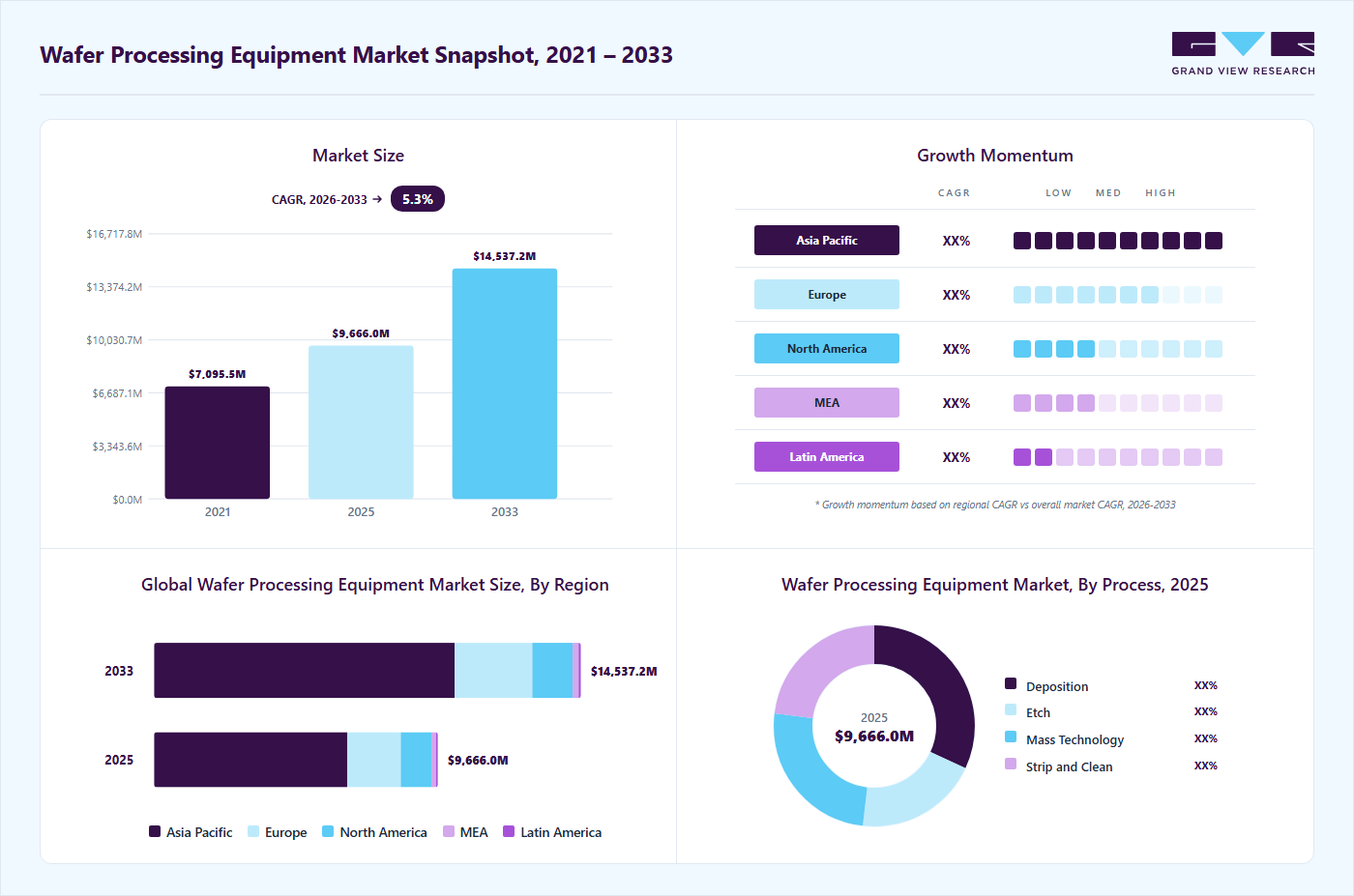
The global wafer processing equipment market size was valued at USD 9.7 billion in 2025 and is projected to grow from USD 10.2 billion in 2026 to USD 14.5 billion by 2033, at a CAGR of 5.2% from 2026 to 2033. The market in Asia Pacific dominated with a revenue share of 68.0% in 2025. This growth is supported by the increasing demand for consumer electronics and the continuous evolution of advanced technologies such as artificial intelligence, 5G connectivity, and autonomous vehicles.
Key Market Trends & Insights
- By process: The deposition segment led the market, capturing the largest revenue share of 31.9% in 2025.
- By application: The sensors segment dominated the market, contributing 40.2% of the total revenue share in 2025.
Regional Highlights
- Largest regional market: Asia Pacific (68.0% revenue share, 2025)
- By country: The China held the largest market share in 2025.
Market Size & Forecast
- Market size in 2025: USD 9.7 Billion
- Estimated market size in 2026: USD 10.2 Billion
- Projected market size by 2033: USD 14.5 Billion
- CAGR (2026-2033): 5.2%
These technologies require high-performance semiconductor devices with greater complexity and precision. Semiconductor manufacturers are expanding advanced fabrication capacity and upgrading production technologies, which is increasing demand for precision wafer processing equipment and supporting overall market growth.The continued miniaturization of electronic devices is a key factor supporting market growth, as it requires the fabrication of increasingly compact and complex integrated circuits. To meet these evolving technical requirements, semiconductor manufacturers are investing in advanced wafer processing equipment capable of delivering higher precision, improved process control, and greater production efficiency. This trend is driving demand for innovative fabrication solutions that can support next-generation chip architectures. The market comprises a diverse range of equipment used in semiconductor wafer fabrication, which forms the foundation of electronic devices such as smartphones, computers, and IoT-enabled systems. As technological advancements accelerate, the need for smaller, faster, and more energy-efficient semiconductor chips continues to increase, further boosting demand for sophisticated processing tools.
")
Moreover, the adoption of advanced manufacturing technologies, including extreme ultraviolet (EUV) lithography and advanced node processing, is enabling the production of ultra-fine circuit patterns, thereby increasing the requirement for next-generation wafer processing equipment. At the same time, growing investments in artificial intelligence infrastructure, high-performance computing, and data centers are contributing to higher semiconductor production volumes. In addition, the global transition toward clean energy, along with the rapid electrification of the automotive sector, is driving demand for power semiconductors used in electric vehicles, renewable energy systems, and industrial automation. These combined trends are expected to support sustained market growth over the forecast period.
Market Concentration & Characteristics
The wafer processing equipment industry shows a high level of consolidation, with a small group of global suppliers accounting for a major share of overall revenue. Established companies maintain strong positions due to their advanced technological capabilities, broad product portfolios, and long-standing relationships with leading semiconductor manufacturers. The industry presents significant barriers to entry, as the development of wafer fabrication equipment requires substantial capital investment, specialized engineering expertise, and lengthy qualification processes before deployment in production environments.
The market is highly technology-driven, with continuous investment in research and development to support advanced semiconductor nodes, EUV lithography, and increasingly complex chip architectures. Equipment integration within fabrication facilities is complex, and switching suppliers involves considerable cost and operational risk, which reinforces long-term partnerships between chipmakers and equipment providers. Demand remains concentrated among a limited number of large semiconductor foundries and integrated device manufacturers, shaping competitive dynamics. Ongoing expansion in artificial intelligence hardware, high-performance computing, and automotive electronics continues to influence product innovation and strategic positioning within the industry.

The competitive environment is also shaped by continuous technological advancement and capacity expansion across major semiconductor manufacturing regions. Equipment suppliers focus on developing solutions that support smaller process nodes, improved yield management, and higher wafer throughput to meet evolving production requirements. The industry also reflects strong collaboration between equipment manufacturers and chipmakers during process development, ensuring compatibility with new materials and architectures. Long equipment lifecycles, recurring service revenue, and aftermarket support further strengthen vendor positioning, while increasing investments in advanced logic, memory, and power semiconductor production continue to sustain demand for established market participants.
Drivers, Opportunities & Restraints
The market is driven by rising demand for advanced semiconductor devices across consumer electronics, data centers, and automotive applications. The growing adoption of artificial intelligence, 5G networks, and Internet of Things technologies is increasing the need for high-performance chips. Semiconductor manufacturers are expanding fabrication capacity and transitioning to advanced process nodes, which is encouraging investments in precision wafer processing equipment. Increasing demand for power semiconductors used in electric vehicles and industrial automation is also contributing to market growth.
Opportunities are emerging from the shift toward advanced packaging, heterogeneous integration, and chip-based architectures that require new processing techniques and specialized equipment. Expanding investments in AI accelerators, high-performance computing infrastructure, and next-generation memory technologies are creating additional demand for advanced fabrication tools. Government initiatives supporting domestic semiconductor manufacturing and the construction of new fabrication facilities across major regions are further opening growth avenues. Rising adoption of compound semiconductors in renewable energy systems and 5G infrastructure also presents new opportunities for equipment providers.
The market faces challenges related to high capital investment requirements and long equipment development cycles. Advanced wafer processing tools involve high costs, which may limit adoption among smaller manufacturers. Supply chain constraints for critical components can impact production schedules and equipment delivery timelines. Rapid technological advancements increase the risk of equipment obsolescence, while cyclical fluctuations in semiconductor demand may lead to delays in capital expenditure by semiconductor companies.
Process Insights
The deposition segment accounted for the largest revenue share of 31.9% in 2025. Deposition plays a fundamental role in semiconductor fabrication, as it involves forming thin films with precise thickness, composition, and uniformity across wafers. The increasing complexity of semiconductor devices and the shift toward smaller technology nodes are driving demand for advanced deposition techniques such as chemical vapor deposition (CVD), physical vapor deposition (PVD), and atomic layer deposition (ALD). These processes enable the creation of multi-layered structures and high-quality films required for improved device performance, power efficiency, and reliability. Growing adoption of 3D architectures, including Fin FET and gate-all-around transistors, is further increasing the importance of highly controlled deposition processes.
The etch process segment also represents a critical stage in wafer fabrication, as it is used to define circuit patterns by selectively removing material from the wafer surface. Etching is essential for forming transistors, contacts, and interconnect structures in advanced integrated circuits. Both dry (plasma) etching and wet chemical etching are widely used, with dry etching gaining greater adoption due to its ability to deliver higher precision, anisotropic profiles, and better process control at advanced nodes. Increasing demand for high-density memory, logic devices, and advanced packaging is driving the need for more sophisticated etch equipment capable of handling complex materials and three-dimensional structures. Continuous improvements in plasma control, selectivity, and process uniformity are further supporting growth in this segment.
Application Insights
The sensors segment held the largest revenue share of 40.2% in 2025. Growth in this segment is supported by increasing deployment of sensors across automotive systems, consumer electronics, healthcare devices, and industrial automation. The expansion of Internet of Things ecosystems and smart connected devices is driving demand for sensors capable of real-time monitoring, environmental detection, and data collection. Semiconductor fabrication for sensors often involves diverse materials and specialized structures, particularly for MEMS devices, image sensors, and environmental sensors. Rising adoption of advanced driver-assistance systems, wearable health devices, and smart manufacturing solutions is further increasing the need for wafer processing equipment optimized for high-precision sensor production.

The memory devices segment continues to represent a significant portion of the market, supported by growing demand for high-speed data storage and processing. Increasing data generation from cloud computing, artificial intelligence workloads, and data centers is driving demand for both volatile and non-volatile memory technologies. Developments in DRAM and NAND flash, including 3D NAND architectures and higher-density memory solutions, are contributing to increased wafer fabrication requirements. Emerging memory technologies and advancements in high-bandwidth memory for AI accelerators are also encouraging investment in advanced wafer processing equipment to support improved performance, capacity, and energy efficiency.
Regional Insights
The wafer processing equipment market in North America is experiencing steady growth, supported by increasing investments in semiconductor research, development, and domestic manufacturing expansion. The region benefits from strong technological infrastructure, a skilled workforce, and the presence of leading semiconductor equipment manufacturers. Growing demand for advanced chips used in artificial intelligence, cloud computing, 5G networks, and automotive electronics is driving the adoption of next-generation fabrication technologies. Expansion of data centers and high-performance computing, along with government initiatives to strengthen semiconductor supply chains, is further contributing to the demand for wafer processing equipment across the region.
U.S Wafer Processing Equipment Market Trends
The wafer processing equipment market in the U.S. is experiencing steady growth, driven by increasing investments in advanced semiconductor manufacturing and technology development. Rising demand for high-performance chips used in artificial intelligence, cloud computing, and data center applications is encouraging semiconductor companies to upgrade fabrication facilities and adopt next-generation wafer processing technologies. The shift toward smaller process nodes and more complex chip architectures is further strengthening demand for precision equipment across logic, memory, and specialty semiconductor production.
Ongoing expansion of domestic semiconductor fabrication capacity is also contributing to market growth, with new facilities focusing on advanced logic, automotive semiconductors, and power devices. The increasing deployment of electric vehicles, advanced driver-assistance systems, and 5G infrastructure is creating additional demand for semiconductor components, thereby supporting equipment investments. Growing adoption of advanced packaging technologies and heterogeneous integration is also influencing the need for specialized wafer processing tools. Moreover, emphasis on supply chain resilience and local manufacturing is encouraging semiconductor companies to strengthen domestic production capabilities. Increasing investments in high-performance computing, AI accelerators, and edge computing devices are further driving demand for sophisticated wafer fabrication equipment. Continuous innovation in materials, process control, and energy-efficient manufacturing is expected to sustain U.S. market growth.
Europe Wafer Processing Equipment Market Trends
The wafer processing equipment market in Europe is witnessing steady growth, supported by increasing investments in semiconductor research, development, and manufacturing capabilities. Regional efforts to strengthen the semiconductor ecosystem and enhance technological innovation are encouraging the adoption of advanced wafer fabrication equipment. The growing demand for semiconductor devices used in automotive electronics, industrial automation, and telecommunications is also contributing to market expansion. The presence of specialized semiconductor companies and research institutions further supports advancements in process technologies and equipment development.
Europe’s strategic focus on improving supply chain resilience and reducing dependence on external semiconductor sources is accelerating investments in local fabrication facilities. Initiatives aimed at expanding domestic chip production and promoting collaboration between industry and research organizations are creating opportunities for equipment suppliers. Rising adoption of electric vehicles, renewable energy systems, and advanced industrial technologies is increasing demand for power semiconductors, which in turn is supporting the growth of wafer processing equipment across the region.
Asia Pacific Wafer Processing Equipment Market Trends
The wafer processing equipment market in the Asia Pacific dominated with the largest revenue share in 2025, supported by its well-established semiconductor manufacturing ecosystem and large-scale fabrication capacity. Countries such as South Korea, China, Japan, and Taiwan play a central role in global chip production, supported by strong electronics manufacturing industries and extensive supply chains. High demand for consumer electronics, smartphones, and computing devices continues to drive semiconductor output in the region. Expansion of 5G infrastructure, artificial intelligence hardware, and automotive electronics production is further increasing the need for advanced wafer processing technologies. Continuous investments in advanced nodes, memory production, and specialty semiconductors are also strengthening regional demand for fabrication equipment.

China wafer processing equipment market is expected to register significant growth over the forecast period, driven by ongoing efforts to expand domestic semiconductor manufacturing capabilities. The country is focusing on increasing local production across logic, memory, and power semiconductor segments to reduce dependence on external suppliers. Large-scale investments in new fabrication facilities and capacity expansion projects are supporting demand for wafer processing equipment. Growth in electric vehicles, renewable energy systems, industrial automation, and consumer electronics manufacturing is also contributing to semiconductor demand. Continued emphasis on supply chain localization, technology development, and expansion of advanced packaging and mature-node production is expected to sustain growth in the Chinese market.
Latin America Wafer Processing Equipment Market Trends
The wafer processing equipment market in Latin America is experiencing moderate growth, supported by the expansion of electronics manufacturing and the increasing adoption of semiconductor-based technologies across automotive, telecommunications, and industrial sectors. Brazil and Mexico are key contributors to regional demand, driven by their growing electronics assembly and automotive production activities. Rising deployment of connected devices, digital infrastructure, and automation solutions is contributing to the demand for semiconductor components, which is encouraging the gradual development of semiconductor processing capabilities. Supply chain diversification and nearshoring strategies are also influencing regional investments, as manufacturers seek to strengthen production networks closer to major end-use markets.
Growing investments in renewable energy systems, electric mobility, and telecommunications infrastructure are further increasing the demand for power semiconductors and advanced electronic components. Argentina and Chile are also witnessing increased adoption of digital technologies, supporting demand for semiconductor devices. This trend is creating opportunities for wafer processing equipment as regional manufacturing and assembly activities continue to expand. Although advanced wafer fabrication capacity remains limited, ongoing improvements in technological infrastructure and collaborations between local manufacturers and global semiconductor companies are expected to support steady market growth in Latin America.
Middle East & Africa Wafer Processing Equipment Market Trends
The wafer processing equipment market in MEA is witnessing gradual growth, supported by increasing investments in digital infrastructure, telecommunications, and emerging technology sectors. The United Arab Emirates, Saudi Arabia, and South Africa are strengthening their semiconductor-related capabilities through research initiatives, technology partnerships, and expansion of electronics manufacturing activities. Growing adoption of smart city projects, 5G deployment, and industrial automation is driving demand for semiconductor components, which is indirectly supporting the need for wafer processing technologies. Expansion of data centers and cloud computing infrastructure across the region is also contributing to demand for advanced chips and related manufacturing equipment.
Rising focus on economic diversification and local technology development is encouraging investments in electronics manufacturing and semiconductor design activities. Increasing adoption of renewable energy systems, electric mobility, and advanced industrial technologies is further boosting demand for power semiconductors. Although large-scale wafer fabrication facilities remain limited, improving technological infrastructure, government-led innovation programs, and collaborations with global semiconductor companies are expected to support the steady market growth in MEA.
Key Wafer Processing Equipment Company Insights
Some of the key players operating in the market include Applied Materials Inc., ASML Holding, Tokyo Electron Limited, Lam Research Corporation, and KLA Corporation, among others.
-
Applied Materials is one of the largest suppliers of wafer processing equipment, offering solutions across deposition, etching, ion implantation, and process control technologies. The company’s equipment is widely used in the fabrication of logic, memory, and power semiconductor devices. It focuses on enabling advanced chip architectures, improving manufacturing efficiency, and supporting emerging applications such as artificial intelligence, high-performance computing, and advanced packaging. Strong research and development capabilities and long-term partnerships with major semiconductor manufacturers contribute to its leading market position.
-
ASML Holding is a leading provider of photolithography systems essential for semiconductor wafer fabrication. The company specializes in deep ultraviolet (DUV) and extreme ultraviolet (EUV) lithography technologies used to produce advanced semiconductor nodes. Its equipment plays a critical role in manufacturing high-performance chips for applications including artificial intelligence, data centers, 5G infrastructure, and consumer electronics. ASML’s focus on innovation and collaboration with major chipmakers has strengthened its position as a key supplier of next-generation semiconductor manufacturing equipment.
Key Wafer Processing Equipment Companies:
The following key companies have been profiled for this study on the wafer processing equipment market.
- Applied Materials, Inc.
- ASML Holding N.V.
- Tokyo Electron Limited
- Lam Research Corporation
- KLA Corporation
- SCREEN Holdings Co., Ltd.
- Hitachi High-Tech Corporation
- ASM International N.V.
- Advantest Corporation
- Canon Inc.
- Nikon Corporation
- Teradyne, Inc.
- Veeco Instruments Inc.
- Kulicke and Soffa Industries, Inc.
- ULVAC, Inc.
Recent Developments
-
In April 2026,Applied Materials, Inc. announced the launch of new deposition systems designed for next-generation semiconductor manufacturing in the angstrom era. The company introduced advanced thin-film deposition tools aimed at enabling chipmakers to produce smaller and more complex transistor structures required for artificial intelligence and high-performance computing applications. These systems enhance material precision, improve process control, and support advanced logic node development, thereby helping semiconductor manufacturers achieve better performance and power efficiency in next-generation chips.
-
In December 2025, Tokyo Electron Limited announced the launch of its EVAROS batch thermal processing system for 300 mm wafers. The newly introduced equipment is designed to enhance productivity by enabling batch processing of multiple wafers while improving temperature uniformity and process stability. The system incorporates advanced thermal control technology to support increasingly complex 3D semiconductor device structures and improve manufacturing efficiency. This launch strengthens the company’s wafer processing equipment portfolio, particularly in thermal processing applications used during semiconductor fabrication.
Wafer Processing Equipment Market Report Scope
Report Attribute
Details
Market size in 2025
USD 9.7 billion
Estimated market size in 2026
USD 10.2 billion
Projected market size by 2033
USD 14.5 billion
Growth rate
CAGR of 5.2% from 2026 to 2033
Historical data
2021 - 2025
Forecast period
2026 - 2033
Quantitative units
Revenue in USD million/billion and CAGR from 2026 to 2033
Report coverage
Revenue forecast, company market position analysis, competitive landscape, growth factors, and trends
Segments covered
Process, application, region
Regional scope
North America; Europe; Asia Pacific; Latin America; MEA
Country Scope
U.S.; Canada; Mexico; UK; Germany; France; Spain; Italy; China; Japan; India; Australia; South Korea; Brazil; Argentina; Saudi Arabia; South Africa; UAE
Key companies profiled
Applied Materials, Inc.; ASML Holding N.V.; Tokyo Electron Limited; Lam Research Corporation; KLA Corporation; SCREEN Holdings Co., Ltd.; Hitachi High-Tech Corporation; ASM International N.V.; Advantest Corporation; Canon Inc.; Nikon Corporation; Teradyne, Inc.; Veeco Instruments Inc.; Kulicke and Soffa Industries, Inc.; ULVAC, Inc.
Customization scope
Free report customization (equivalent up to 8 analysts working days) with purchase. Addition or alteration to country, regional & segment scope.
Pricing and purchase options
Avail customized purchase options to meet your exact research needs. Explore purchase options
Global Wafer Processing Equipment Market Report Segmentation
This report forecasts revenue growth at global, regional & country levels and provides an analysis of the industry trends in each of the sub-segments from 2021 to 2033. For this study, Grand View Research has segmented the global wafer processing equipment market report based on the process, application, and region:

-
Process Outlook (Revenue, USD Million; 2021 - 2033)
-
Deposition
-
Etch
-
Mass Technology
-
Strip and Clean
-
-
Application Outlook (Revenue, USD Million, 2021 - 2033)
-
Memory Devices
-
Logic Devices
-
Analog Devices
-
Sensors
-
-
Regional Outlook (Revenue, USD Million, 2021 - 2033)
-
North America
-
U.S.
-
Canada
-
Mexico
-
-
Europe
-
UK
-
Germany
-
France
-
Italy
-
Spain
-
-
Asia Pacific
-
Japan
-
China
-
India
-
Australia
-
South Korea
-
-
Latin America
-
Brazil
-
Argentina
-
-
Middle East & Africa
-
South Africa
-
Saudi Arabia
-
UAE
-
-
Frequently Asked Questions About This Report
The deposition segment led with a 31.9% revenue share in 2025.
The sensors held the largest revenue share of 40.2% in 2025.
The wafer processing equipment market is primarily driven by the relentless demand for advanced semiconductor chips, fueled by the rapid proliferation of consumer electronics, such as smartphones, tablets, and wearable devices. Additionally, the advent of cutting-edge technologies, including 5G, Internet of Things (IoT), artificial intelligence (AI), and electric vehicles, necessitates the development of more sophisticated, high-performance semiconductor devices. This, in turn, requires the use of advanced wafer processing equipment capable of manufacturing smaller, faster, and more energy-efficient chips, thereby driving market growth.
The global wafer processing equipment market size was valued at USD 9.7 billion in 2025 and is expected to reach USD 10.2 billion in 2026.
The global wafer processing equipment market, in terms of revenue, is expected to grow at a compound annual growth rate of 5.2% from 2026 to 2033 to reach USD 14.5 billion by 2033.
Asia Pacific dominated the wafer processing equipment market with a revenue share of 68.0% in 2025.
Key players include Applied Materials, Inc.; ASML Holding N.V.; Tokyo Electron Limited; Lam Research Corporation; KLA Corporation; SCREEN Holdings Co., Ltd.; Hitachi High-Tech Corporation; ASM International N.V.; Advantest Corporation; Canon Inc.; Nikon Corporation; Teradyne, Inc.; Veeco Instruments Inc.; Kulicke and Soffa Industries, Inc.; ULVAC, Inc.
About the Author(s)
Advanced Interior Materials Research Team
Advanced Materials · Advanced Interior MaterialsThis report was authored by the advanced interior materials research team at Grand View Research - comprising two research analysts, one senior research analyst, and one industry expert - with specialized expertise in the advanced interior materials segment of the advanced materials industry. All findings are based on proprietary advanced materials databases, executive interviews, and regulatory analysis, subject to internal peer review prior to publication.
Last Updated:
Speak to Analyst


Need a Tailored Report?
Customize this report to your needs — add regions, segments, or data points, with 20% free customization.
Or view our licence options:

ISO 9001:2015 & 27001:2022 Certified
We are GDPR and CCPA compliant! Your transaction & personal information is safe and secure. For more details, please read our privacy policy.